Field effect transistor multi-layer field plate device and method for making the same

A field effect transistor and field plate technology, applied in the field of microwave power devices, can solve the problems of increasing the length of the depletion region and decreasing the gain, and achieve the effects of suppressing current collapse, improving breakdown characteristics and eliminating current collapse.

Inactive Publication Date: 2008-07-30
INST OF MICROELECTRONICS CHINESE ACAD OF SCI
View PDF0 Cites 40 Cited by
  • Summary
  • Abstract
  • Description
  • Claims
  • Application Information

AI Technical Summary

Problems solved by technology

[0018] However, the addition of the gate connection field plate increases the capacitance between the gate and drain, and also increases the length of the depletion region, resulting in a decrease in gain

Method used


Image

  • Field effect transistor multi-layer field plate device and method for making the same
  • Field effect transistor multi-layer field plate device and method for making the same
  • Field effect transistor multi-layer field plate device and method for making the same

Examples


Embodiment Construction

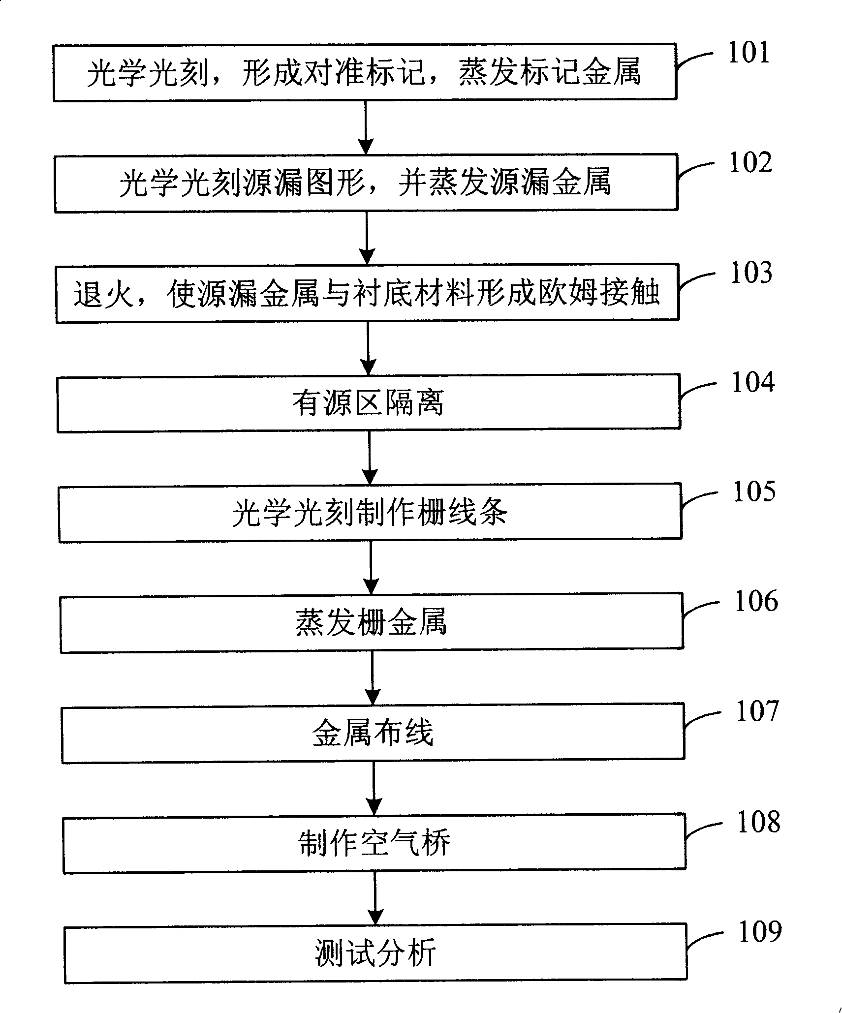
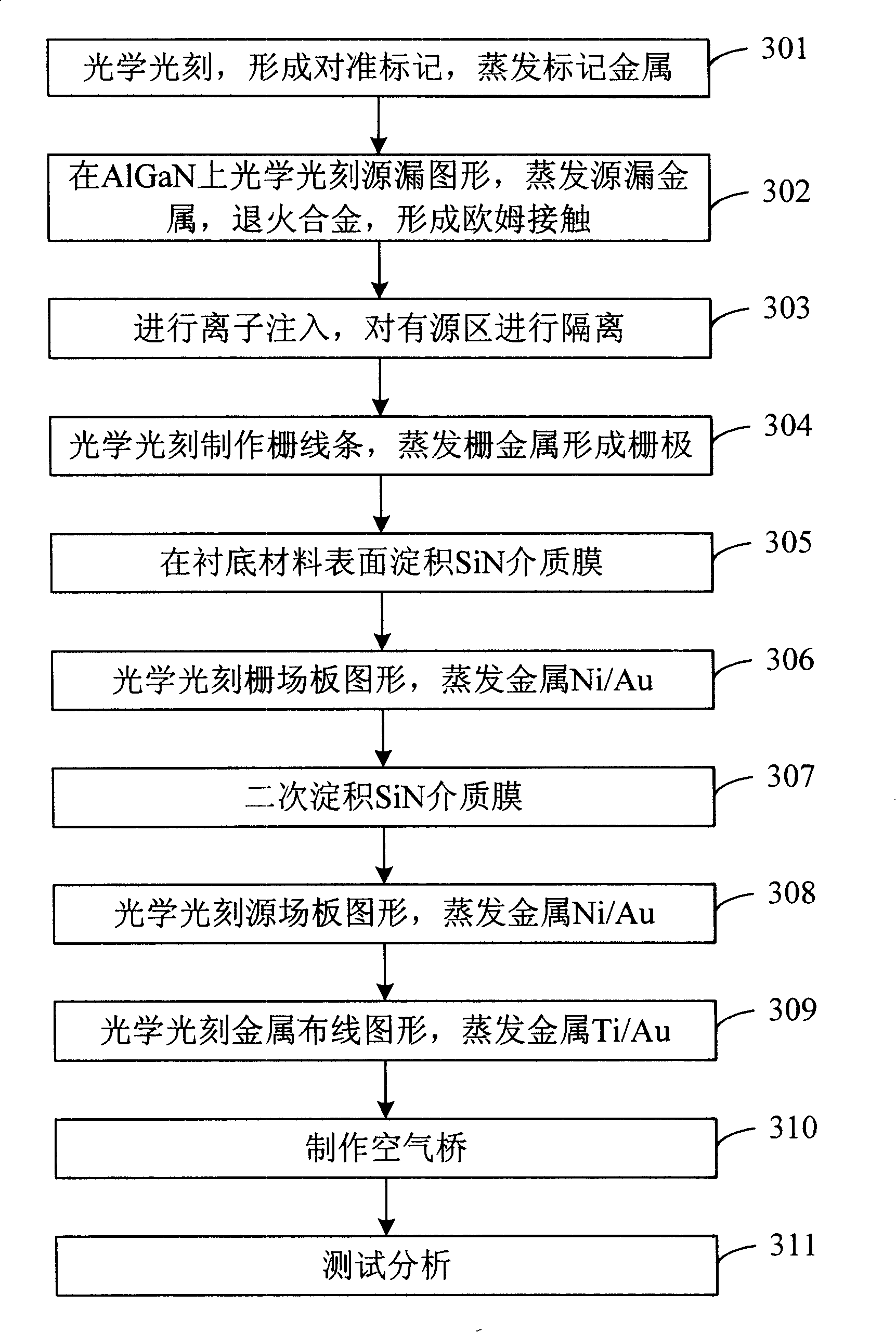
[0056] In order to make the object, technical solution and advantages of the present invention clearer, the present invention will be described in further detail below in conjunction with specific embodiments and with reference to the accompanying drawings.

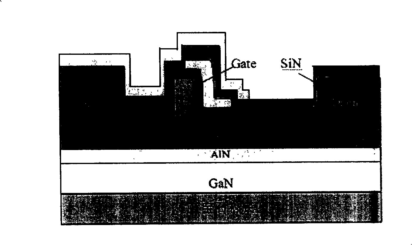
[0057] Such as figure 2 as shown, figure 2 A schematic structural diagram of an AlGaN / GaN HEMT multilayer field plate device provided by the present invention. The AlGaN / GaN HEMT multilayer field plate device includes:

[0058] gate, source and drain on either side of the gate; where,

[0059] The gate, source and drain are located on the top aluminum gallium nitride (AlGaN) epitaxial layer of the substrate material, and an ohmic contact is formed between the source and the AlGaN epitaxial layer and the drain and the AlGaN epitaxial layer through an annealing alloy;

[0060] Deposit a SiN dielectric film on the surface of the device where the gate, source and drain are formed, and evaporate the pattern of the gate co...


PUM


Abstract

The invention relates to the field of microwave power device technology in semiconductor material and discloses a method for fabricating an AlGaN/GaN high-electron mobility transistor (AlGaN/GaN HEMT) multilayer field plate device. The method comprises, based on common AlGaN/GaN HEMT device fabrication process, firstly fabricating a gate connection field plate after forming a gate metal contact, secondly fabricating a source connection field plate, and forming the AlGaN/GaN HEMT multilayer field plate device. The invention simultaneously discloses an AlGaN/GaN HEMT multilayer field plate device. The invention can greatly improve the breakdown characteristics of the AlGaN/GaN HEMT device and effectively suppress the current collapse of the AlGaN/GaN HEMT device.

Description

technical field [0001] The invention relates to the technical field of microwave power devices in semiconductor materials, in particular to an aluminum gallium nitride / gallium nitride high electron mobility field effect transistor (AlGaN / GaN HEMT) multilayer field plate device and a manufacturing method thereof. Background technique [0002] Gallium nitride (GaN), as the third-generation wide-bandgap semiconductor material, has a large bandgap (3.4eV), a high breakdown voltage (3.3MV / cm), and a high two-dimensional electron gas concentration (greater than 10 13 cm 2 ), high velocity of saturated electrons (2.8×10 7 cm / s) and other characteristics have received extensive attention internationally. [0003] At present, the high frequency, high voltage, high temperature and high power characteristics of AlGaN / GaN HEMT devices make them have great prospects in microwave power devices. [0004] For conventional AlGaN / GaN HEMT devices, the usual process steps are as follows fi...

Claims


Application Information

Patent Timeline
Patent Type & Authority Applications(China)
IPC IPC(8): H01L29/778H01L21/335
Inventor 刘果果刘新宇郑英奎魏珂
Owner INST OF MICROELECTRONICS CHINESE ACAD OF SCI
Why Eureka
Try Eureka