Photovoltaic application of amorphous germanium thin film

A technology of amorphous germanium and amorphous silicon germanium, applied in the field of multi-junction photovoltaic devices based on amorphous silicon, can solve the problems of high price

Inactive Publication Date: 2008-08-20
BEIJING XINGZHE MULTIMEDIA TECH
View PDF2 Cites 14 Cited by
  • Summary
  • Abstract
  • Description
  • Claims
  • Application Information

AI Technical Summary

Problems solved by technology

The production of high-performance triple-junction a-Si/a-SiGe/a-SiGe photovoltaic modules must us

Method used


Image

  • Photovoltaic application of amorphous germanium thin film
  • Photovoltaic application of amorphous germanium thin film
  • Photovoltaic application of amorphous germanium thin film

Examples


Embodiment 1

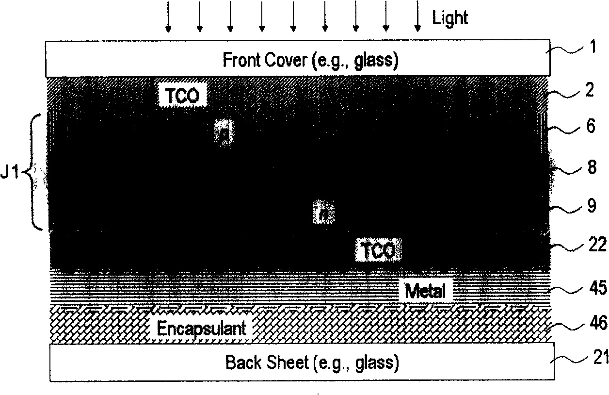
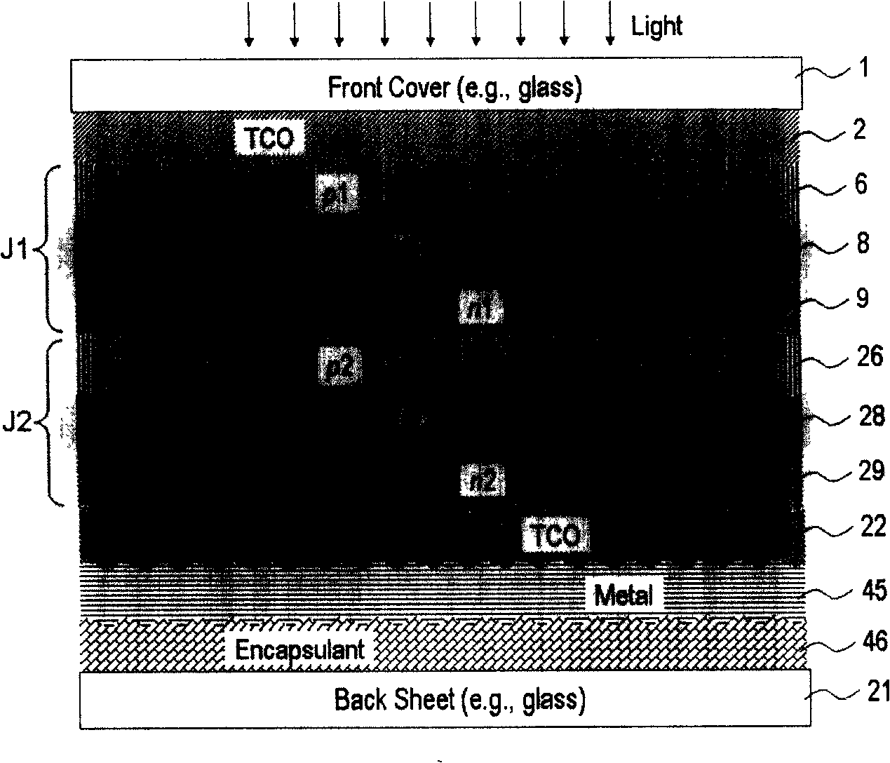
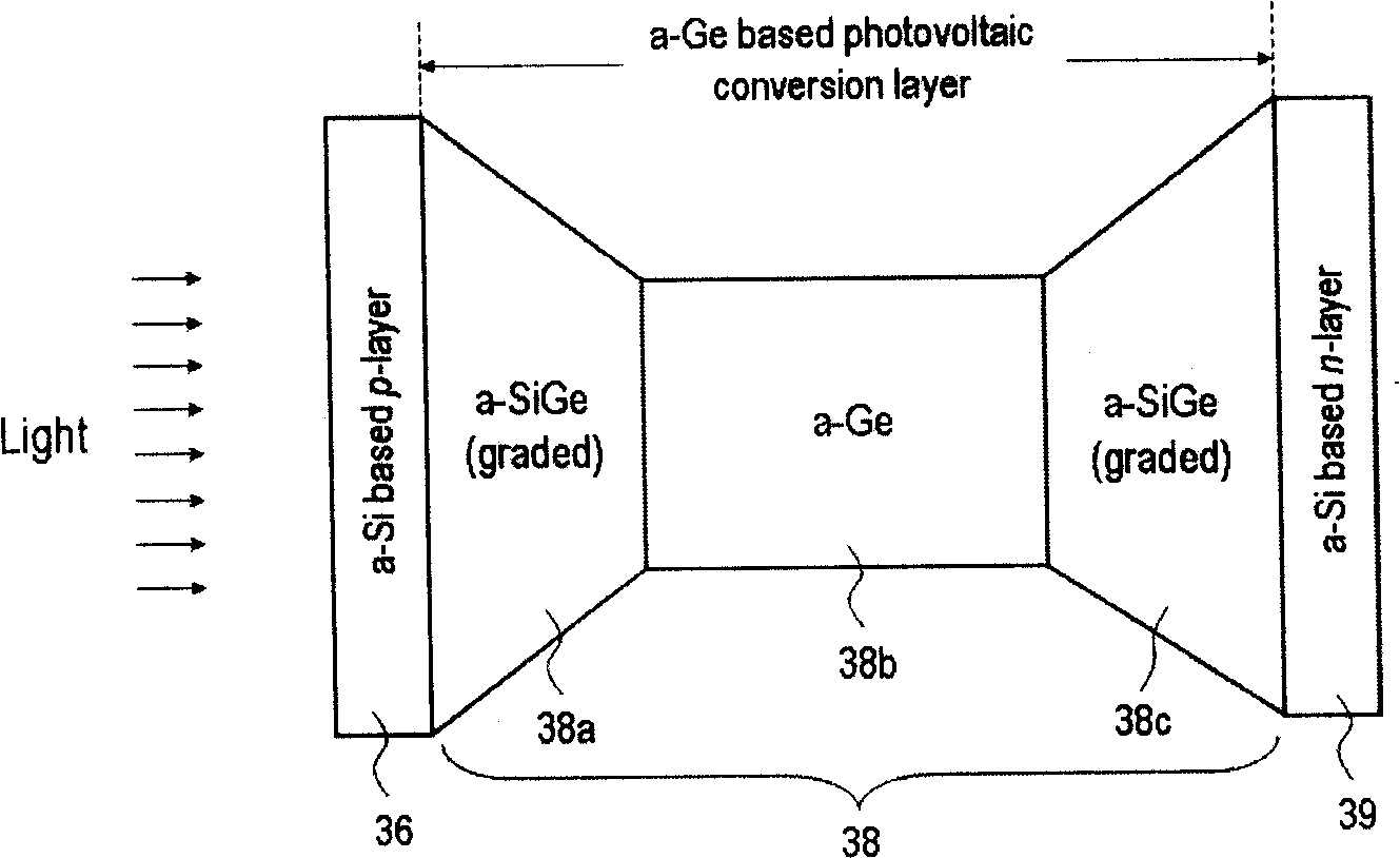
[0034] like Figure 4 As shown, the first example is a triple-junction photovoltaic cell, and its detailed film structure is as follows Image 6 shown. The triple-junction photovoltaic cell includes a top junction J1 made of amorphous silicon, a middle junction J2 made of nanocrystalline silicon and a bottom junction J3 made of amorphous silicon germanium (a-Si / nc-Si / a-Ge). They are also called the first knot, the second knot and the third knot respectively, and represent Image 6 The p-i-n sequences 6-8-9, 26-28-29 and 36-38-39 in . The advantage of this combination of different intrinsic layers is that each photovoltaic cell can be produced relatively quickly. The intrinsic layer 8 of amorphous silicon of the top junction J1 is only 700nm thick and can be easily deposited, and it is used to absorb blue light. The nanocrystalline silicon intrinsic layer 28 of the second junction cell J2 needs to absorb green light and some red light to generate enough photocurrent to coop...

Embodiment 2

[0037] Figure 5 is another example of a triple junction photovoltaic cell where the third junction (bottom junction) contains an intrinsic layer of amorphous germanium. The detailed film structure of the device is as follows Figure 7 shown. It includes an interlayer R1 made of transparent conductive oxide (TCO) ZnO, placed between the second junction J2 and the third junction J3. The p-i-n configurations of photovoltaic units J1, J2 and J3 are 6-8-9, 26-28-29, 36-38-39 respectively, such as Figure 7 shown. Mezzanine R1 (such as Figure 7 32) has the effect of generating an abrupt index of refraction at the interface between the silicon-based thin film and the TCO, so that unabsorbed light is reflected into the second junction photovoltaic cell J2. The first junction and the second junction of the device described in this example are made of amorphous silicon with an energy band gap between 1.8-1.7eV, while the third junction is made of amorphous germanium and related b...


PUM

PropertyMeasurementUnit
Thicknessaaaaaaaaaa
Thicknessaaaaaaaaaa
Thicknessaaaaaaaaaa

Abstract

The present invention discloses a multi-junction photovoltaic device with simpler structure and lower cost. The multi-junction photovoltaic device comprises of first junction, second junction and third junction based on silicon film photovoltaic cell with folding structure. The third cell intrinsic i layer comprises of at least one amorphous germanium film whose band gap is less than 1.1eV, and buffer layer containing grads band gap amorphous germanium silicon alloy and/or film based on nano crystal silicon. The multi-junction photovoltaic device containing amorphous germanium has good capability and can be produced by low cost equipment.

Description

technical field [0001] The invention relates to a multi-junction thin film photovoltaic device and its production method. In particular, it relates to multi-junction photovoltaic devices based on amorphous silicon, which have better power efficiency and stability. The invention relates to a multi-junction photovoltaic device with simpler structure and lower production cost. Background technique [0002] In recent years, the development of photovoltaic cells and large-area photovoltaic modules has attracted widespread attention in the world. Hydrogenated amorphous silicon and nanocrystalline silicon, in particular, have shown great potential with the widespread adoption of photovoltaic devices in commercial and residential installations. A remarkable feature of producing thin-film silicon photovoltaic devices at a temperature lower than 260°C is that low cost and high performance can be achieved at the same time. This is because silicon-based semiconductor layers and elect...

Claims


Application Information

Patent Timeline
IPC IPC(8): H01L31/075H01L31/042H01L31/0376H01L31/076
CPCY02E10/52Y02E10/548
Inventor 李沅民马昕
Owner BEIJING XINGZHE MULTIMEDIA TECH
Why Eureka
Try Eureka