Trace amount of boron doped intrinsic silicon hydride thin film

A technology of hydrogenated silicon and thin films, applied in the field of solar energy materials, can solve problems such as difficult extraction and performance impact

Inactive Publication Date: 2008-08-20
BEIJING XINGZHE MULTIMEDIA TECH
View PDF0 Cites 3 Cited by
  • Summary
  • Abstract
  • Description
  • Claims
  • Application Information

AI Technical Summary

Problems solved by technology

So the usual so-called undoped or "intrinsic" i-type silicon hydrogenated thin films don't really have intrinsic properties, because the Fermi level in this material is located above the middle of the bandgap, making The holes (minority carriers) are not easily extracted, which affects the performance of this material as an i-layer in p-i-n batteries

Method used


Image

  • Trace amount of boron doped intrinsic silicon hydride thin film

Examples


Embodiment Construction

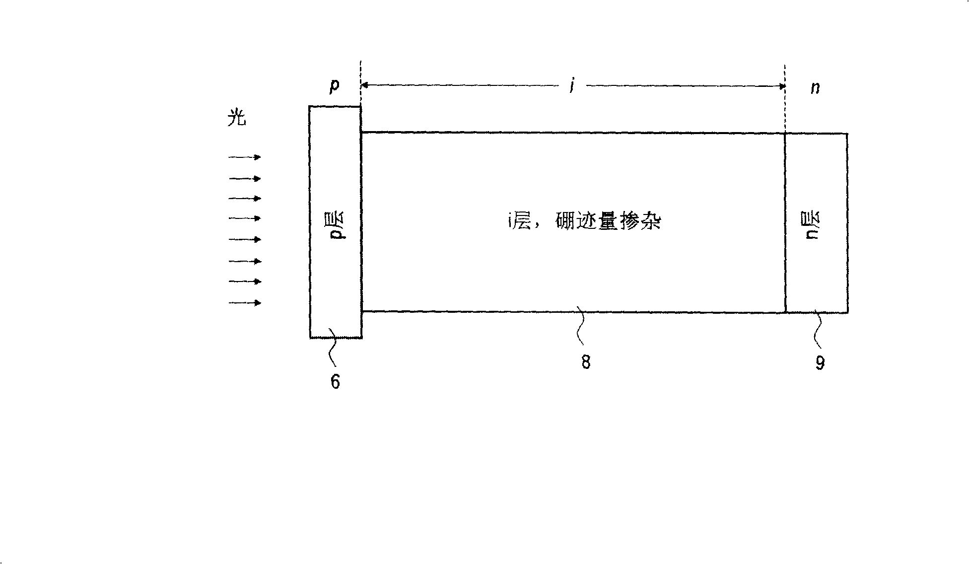
[0010] As shown in the accompanying drawings, a p-i-n type solar cell based on a hydrogenated silicon thin film sequentially contains a p-layer 6 based on hydrogenated silicon or its alloy with a boron doping degree of not less than 0.2%, a "non-doped" hydrogenated silicon The i-layer 8 and an n-layer 9 based on hydrogenated silicon or an alloy thereof with a phosphorus doping degree of not less than 0.5%. When using the plasma enhanced chemical vapor deposition method to form the hydrogenated silicon i-layer 8, the substrate temperature used does not exceed 230°C, and a trace amount of boron-containing gas is added to the provided source gas mixture containing the silicon-containing gas. , the ratio of boron-containing gas to silicon-containing gas does not exceed 2ppm. Not less than 90% of the source gas mixture is hydrogen, and the silicon-containing gas is silane. When the source gas mixture is mainly high-purity hydrogen and silane (purity not less than 99.999%), the opt...


PUM


Abstract

The present invention discloses a method for making the hydrogenated Si containing hydrogenated amorphous silicon and hydrogenated nanocrystalline silicon has real intrinsic capability. In process of plasma enhanced chemical vapor deposition, adding a certain gas containing boron to mixture of hydrogen and silane, making boron counteract doping effect of inevitably n-type impurity. The hydrogenated Si film gained by this method, can improve conversion efficiency and stability of p-i-n type photovoltaic device.

Description

technical field [0001] The invention belongs to the scope of solar energy materials, and particularly relates to the formation technology of hydrogenated silicon thin films. Background technique [0002] Solar photovoltaic power generation is one of the important ways to obtain renewable energy that is beneficial to the environment. Therefore, in recent years, the development of photovoltaic cells and large-area photovoltaic modules has attracted widespread attention in the world. Thin-film solar cells represent a trend in photovoltaic technology, especially hydrogenated amorphous silicon and nanocrystalline silicon, which show great potential with the widespread application of photovoltaic devices in commercial and residential facilities. A notable feature of producing thin-film silicon photovoltaic devices at lower temperatures below 260°C is the superior performance of large-area deposition of silicon-related semiconductor layers and electrical contact layers. At the sam...

Claims


Application Information

Patent Timeline
Patent Type & Authority Applications(China)
IPC IPC(8): H01L31/18H01L21/205
CPCY02P70/50
Inventor 李沅民马昕
Owner BEIJING XINGZHE MULTIMEDIA TECH
Why Eureka
Try Eureka