Light emitting diode and laser and its production method

A technology of light-emitting diodes and manufacturing methods, which is applied to lasers, laser components, semiconductor lasers, etc., can solve problems such as inability to prepare high-performance and cracks in thin-film materials, and achieve the effects of reducing substrate costs and improving luminous efficiency

Inactive Publication Date: 2008-08-20
NANKAI UNIV
View PDF1 Cites 4 Cited by
  • Summary
  • Abstract
  • Description
  • Claims
  • Application Information

AI Technical Summary

Problems solved by technology

The research on using bulk silicon substrates to make GaN LEDs has also attracted people's attention recently (Selective area deposited blue GaN-InGaN multiple-quantum well light emitting diodes over silicon substrates, J.W.Yang, A.Lunev, G.Simin, A.Chitnis, M. Shatalov, and M.AsifKhan, APPLIED PHYSICS LETTERS VOLUME 76, NUMBER 3, 273, 2000), the difficulty lies in: the thermal mismatch and lattice mismatch between Si and GaN-type materials will lead to the tortoise of GaN-type thin film materials In addition, the bulk silicon substrate is opaque in the visible light range, which requires the LED to adopt a top-emitting structure, and 50% of the photons emitted from the GaN active layer have the potential to be absorbed by the bulk silicon substrate

Method used


Image

  • Light emitting diode and laser and its production method
  • Light emitting diode and laser and its production method
  • Light emitting diode and laser and its production method

Examples


Embodiment Construction

[0054] The manufacturing method of the light-emitting diode and the laser, as well as the light-emitting diode and the laser of the present invention will be described in detail below with reference to the embodiments and the accompanying drawings.

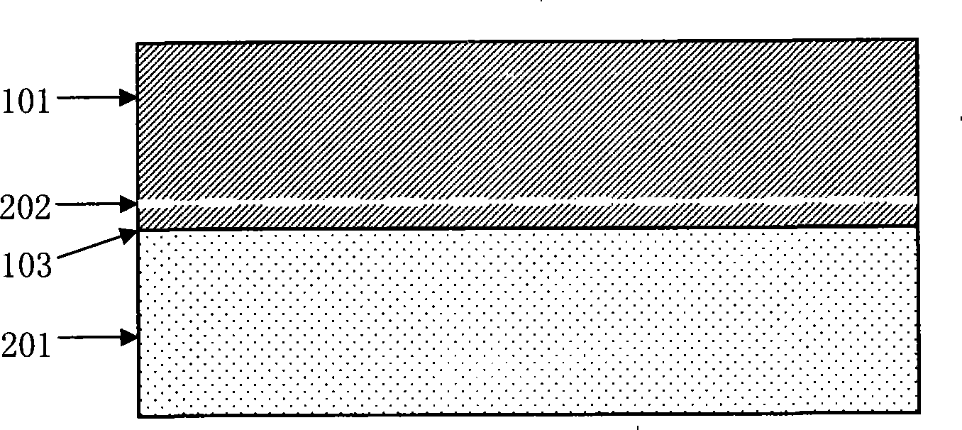
[0055] The manufacturing method of semiconductor light-emitting diode (LED) and laser (LD) of the present invention, described light-emitting diode and semiconductor laser are direct epitaxial growth on single crystal silicon thin-film quartz (SOQ) substrate or epitaxial growth is deposited on buffer layer on single crystal silicon thin film quartz (SOQ) substrates.

[0056] The manufacturing method of semiconductor light-emitting diode and laser of the present invention specifically comprises the following steps:

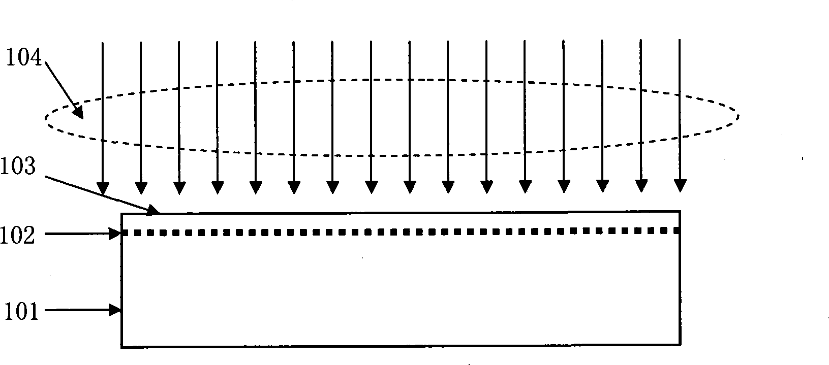
[0057] (1) Chemical-mechanical polishing (CMP) of the single crystal silicon wafer reaches a set thickness, the set thickness is 100nm-300nm, and then large-dose hydrogen ion implantation is performed within the set th...


PUM


Abstract

The present invention provides a LBD, a laser and a producing method thereof. Epitaxial growth of LBD and laser on single crystal silicon film quartz substrate or single crystal silicon film quartz substrate deposited buffer layer. Semiconductor LBD structure comprises of single crystal silicon film bonded quartz substrate, single silicon film electrode layer formed on quartz substrate, N layer epitaxial grown on LED of single silicon electrode layer and LED top electrode formed on P layer. Semiconductor laser structure comprises of single crystal silicon bonded quartz substrate, single crystal silicon electrode layer formed on quartz substrate, N layer epitaxial grown on LD of single crystal silicon electrode layer, active layer of LD on N layer, P layer of LD on LD active layer and top electrode of LD on P layer of LD. The present invention can realize bottom luminescence of LED and LD elements, improve luminescence efficiency of LED and LD.

Description

technical field [0001] The invention relates to a semiconductor light emitting diode and a semiconductor laser. In particular, it relates to a manufacturing method of a light-emitting diode and a laser for epitaxially growing a semiconductor light-emitting diode and a semiconductor laser on a single-crystal silicon thin-film quartz substrate, and the light-emitting diode and the laser. Background technique [0002] At present, GaN-based light-emitting diodes (LEDs) are usually fabricated on sapphire (Al 2 o 3 ) (S. Nakamura, T. Mukai, and M. Senoh, Appl. Phys. Lett., 64, 1687, 1994) or on a silicon carbide (SiC) substrate (GROUPIII NITRIDE LED WITH SILICON CARBIDE SUBSTRATE, Edmond, John Adam ; Doverspike, Kathleen Marie; Kong, Hua-shuang; Bergmann, Michael John; U.S. Patent, 20050040426) they have substrates that are relatively expensive, and the diameter of the substrate is usually only 2-4 inches, which cannot be compared with mature silicon (Si) microelectronics Circu...

Claims


Application Information

Patent Timeline
Patent Type & Authority Applications(China)
IPC IPC(8): H01L33/00H01S5/00
Inventor 孟志国吴春亚熊绍珍李娟
Owner NANKAI UNIV
Why Eureka
Try Eureka