Resistive random access memory and manufacturing method for the same

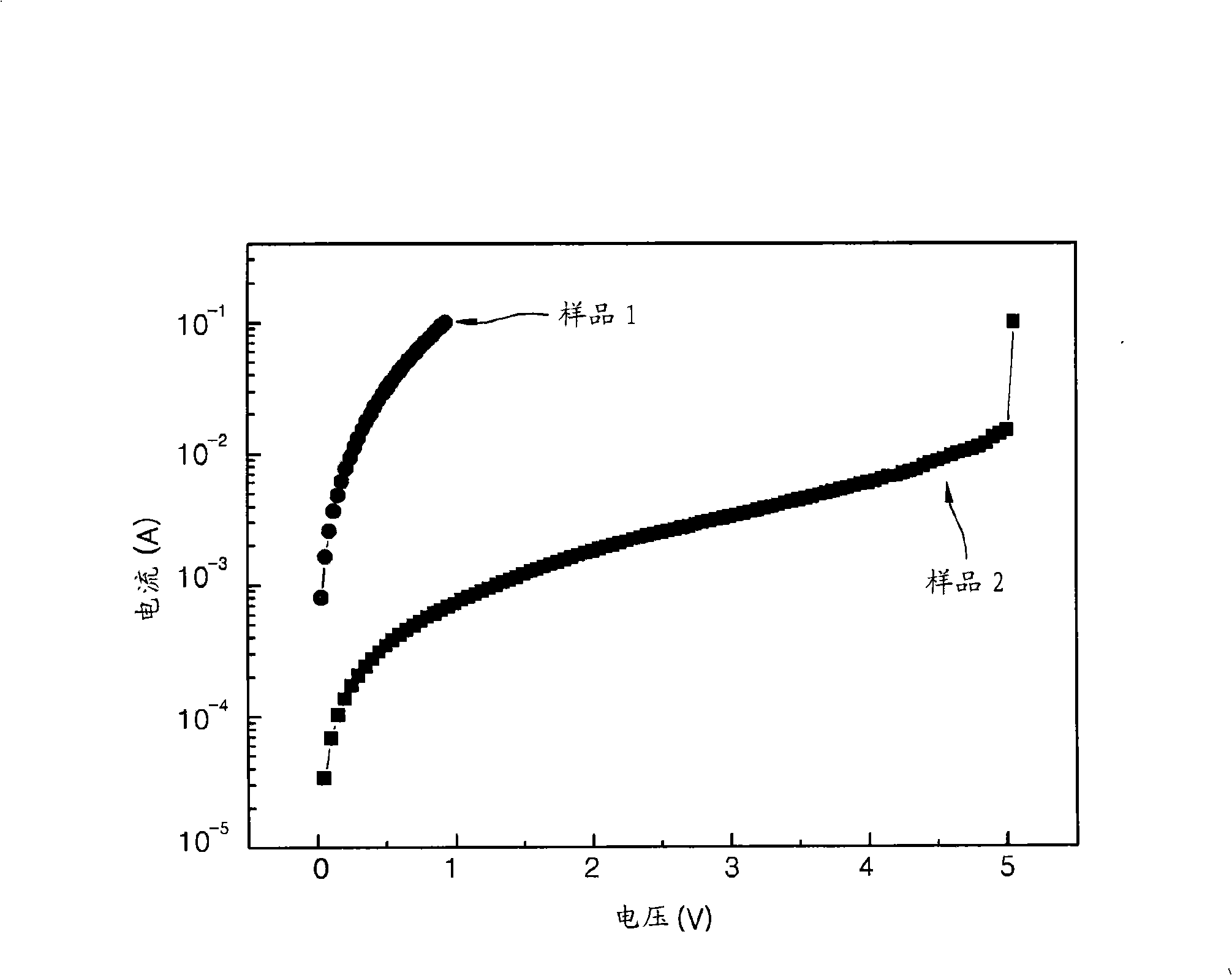
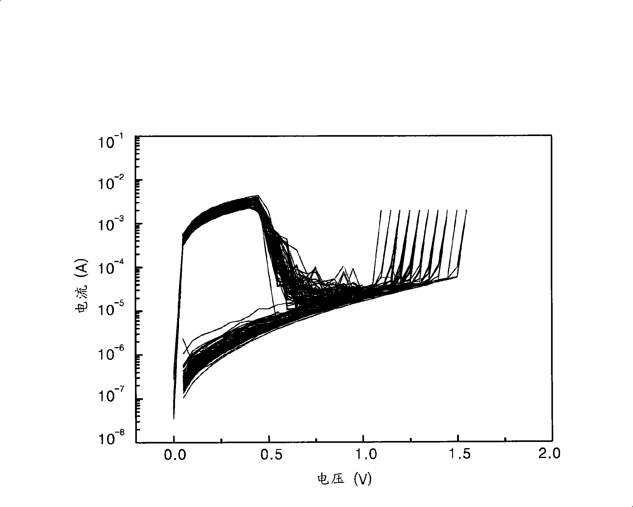
一种随机存取存储器、电阻的技术,应用在静态存储器、只读存储器、数字存储器信息等方向,能够解决样品1不能作为RRAM使用、样品1不具有可变电阻特性等问题

Inactive Publication Date: 2008-09-03
SAMSUNG ELECTRONICS CO LTD
View PDF2 Cites 7 Cited by
  • Summary
  • Abstract
  • Description
  • Claims
  • Application Information

AI Technical Summary

Problems solved by technology

[0011] Because sample 1 is deposited at a lower temperature, sample 1 does not have variable resistance characteristics, so sample 1 cannot be used as RRAM

Method used


Image

  • Resistive random access memory and manufacturing method for the same
  • Resistive random access memory and manufacturing method for the same
  • Resistive random access memory and manufacturing method for the same

Examples


example 1

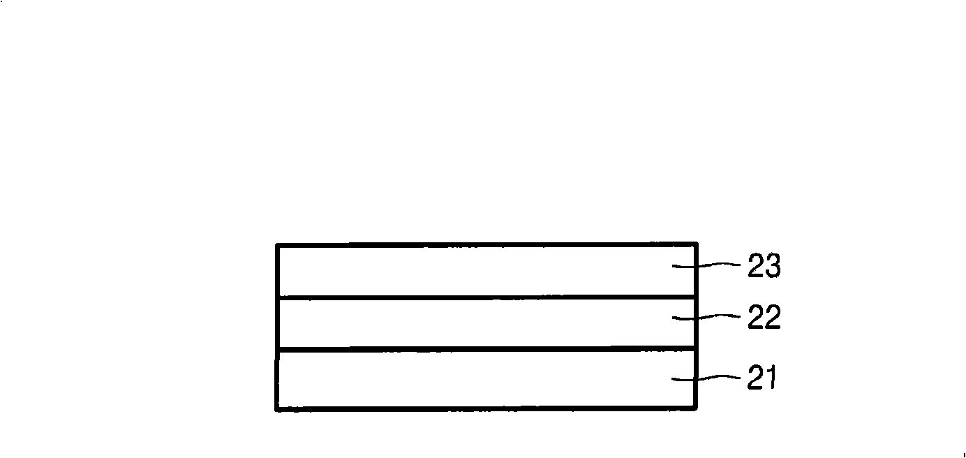
[0053] Example 1: RRAM comprising a NiO layer with 0.05 wt% titanium ions

[0054] A platinum electrode with a thickness of 50 nm was formed on the substrate. Thickness is A NiO layer with a size of 100 μm × 100 μm with 0.05 wt% titanium ions was formed on the platinum electrode by using a reactive sputtering method using doped with 0.05 wt% titanium ions (O 2 Partial pressure: 10 mol %, sputtering temperature: room temperature of about 25° C.) Ni target. Then, platinum electrodes were formed on the NiO layer with 0.05wt% titanium ions to provide RRAM.

example 2

[0055] Example 2: RRAM comprising a NiO layer with 0.1 wt% titanium ions

[0056] The RRAM was fabricated in the same manner as in Example 1, except that a NiO layer with 0.1 wt% titanium ions was formed using a nickel target doped with 0.1 wt% titanium ions instead of the nickel target doped with 0.05 wt% titanium ions.


PUM


Abstract

Provided are a resistance random access memory including a resistance layer having a metal oxide and / or a metal ion dopant, which may be deposited at room temperature and which may have variable resistance characteristics, and a method of manufacturing the same.

Description

technical field [0001] The present invention relates to a resistive random access memory (RRAM) comprising a resistive layer with metal oxide and / or metal ion dopants and a method of manufacturing the same. The resistance layer of the RRAM can be formed at a lower temperature and can have better electrical characteristics, and thus, the RRAM including the resistance layer can be more reliable and manufactured in a more cost-effective manner. Background technique [0002] Semiconductor memory arrays include many memory cells connected in circuits. In a dynamic random access memory (DRAM), which is an example of a semiconductor memory device, a unit memory cell is composed of a switch and a capacitor. The advantage of DRAM is that DRAM has a higher degree of integration and operates at a faster speed. However, when the power to the DRAM is interrupted, all data stored in the DRAM is lost. [0003] A flash memory device is an example of a nonvolatile memory device in which d...

Claims


Application Information

Patent Timeline
Patent Type & Authority Applications(China)
IPC IPC(8): H01L45/00H01L27/24G11C13/00G11C11/56G11C16/02
CPCH10B63/30H10N70/20H10N70/826H10N70/8833H10N70/026H10B99/00
Inventor 李明宰李殷洪朴泳洙
Owner SAMSUNG ELECTRONICS CO LTD
Why Eureka
Try Eureka