Anisotropically conductive member and method of manufacturing the same
A technology of anisotropy and manufacturing method, applied in the direction of electrical component connection, cable/conductor manufacturing, electrical components, etc., can solve the problem of difficulty in reducing the size of the conduction path, achieve high-efficiency manufacturing, reduce positioning load, improve Set the effect of density
- Summary
- Abstract
- Description
- Claims
- Application Information
AI Technical Summary
Problems solved by technology
Method used
Image

Examples
Embodiment 1
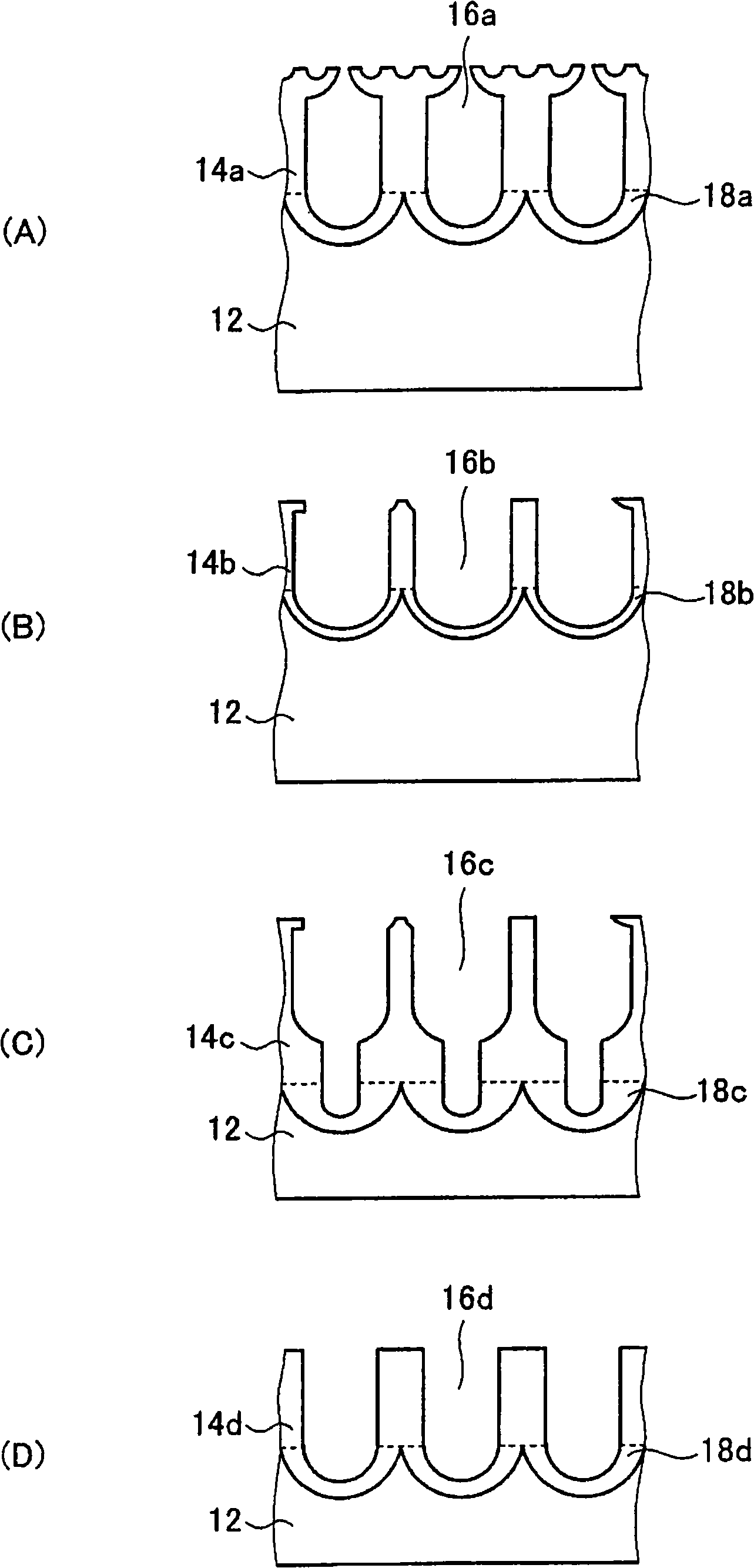
[0310] (A) Mirror polishing treatment (electrolytic polishing treatment)
[0311] A high-purity aluminum substrate (manufactured by Sumitomo Light Metal Co., Ltd., purity 99.99% by mass, thickness 0.4 mm) was cut into an area of 10 cm square for anodic oxidation treatment, and an electrolytic polishing liquid with the following composition was used at a voltage of 25 V and a liquid temperature of 65 ° C. , Under the condition of a liquid flow rate of 3.0m / min, the electrolytic grinding process was implemented.
[0312] A carbon electrode was used as a cathode, and GP0110-30R (manufactured by Takasago Seisakusho Co., Ltd.) was used as a power supply. In addition, the flow rate of the electrolytic solution was measured using a vortex flow rate monitor FLM22-10PCW (manufactured by AS ONE).
[0313] (Electrolytic polishing liquid composition)
[0314] ・85% by mass phosphoric acid (reagent manufactured by Wako Pure Chemical Industries, Ltd.): 660 mL
[0315] ·Pure water: 160mL...
Embodiment 2
[0341] After each treatment of (A) to (G) was performed in the same manner as in Example 1, a treatment of covering copper protruding from the surface of the insulating base material (anodized film) with gold was performed.
[0342] Specifically, by immersing the trimmed anisotropic conductive member obtained in Example 1 for 15 minutes in a commercially available electroless plating solution (presia suhabu) maintained at 50° C., gold was precipitated on the insulating surface. The substrate protrudes from the surface of the copper.
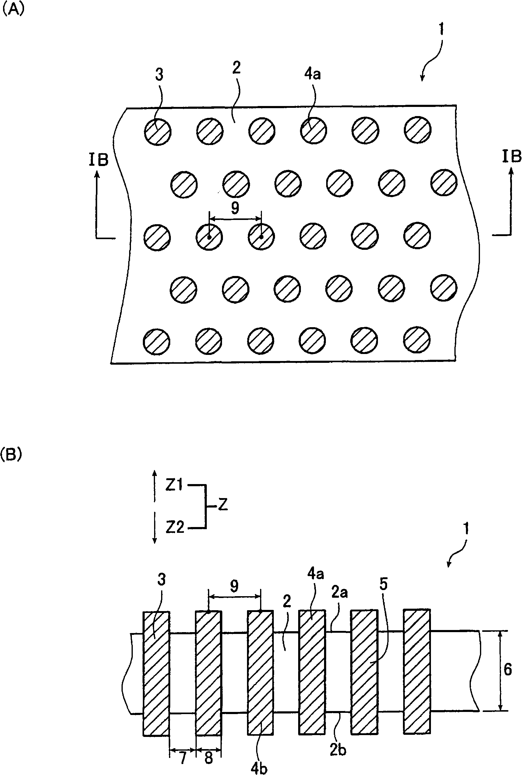
[0343] When observed with FE-SEM in the same manner as in Example 1, the protruding portion was rounded, and the protrusion height increased to about 20 nm. In addition, as shown in Table 1 below, it was confirmed that the diameter of the conduction path, which is the size of the electrode portion, was 40 nm, and the thickness of the member was 50 μm. In addition, it was confirmed that the length (length / thickness) of the center line of the cond...
Embodiment 3
[0345] In addition to changing the anodic oxidation and re-anodized treatment in the above (B) anodic oxidation treatment process (self-regularization method I), it was changed to an electrolyte solution of 0.50mol / L oxalic acid, with a voltage of 40V, a liquid temperature of 15°C, and a liquid flow rate of 3.0m / min, except that the treatment time of the above (G) trimming treatment was set to 10 minutes, the treatment was carried out under the same conditions as in Example 1 to obtain a structure (anisotropic conductive member).
[0346] When observed with FE-SEM in the same manner as in Example 1, as shown in Table 1 below, it was confirmed that the height of the protrusion was 40nm, the size of the electrode part, that is, the diameter of the conduction path, was 120nm, and the thickness of the part was 50μm. In addition, it was confirmed that the length (length / thickness) of the center line of the conduction path relative to the thickness of the member was 1.01.
PUM
| Property | Measurement | Unit |
|---|---|---|
| Thickness | aaaaa | aaaaa |
| Diameter | aaaaa | aaaaa |
| Thickness | aaaaa | aaaaa |
Abstract
Description
Claims
Application Information