Structure for testing integrality of grid medium layer, forming method and test method thereof

A gate dielectric layer and test structure technology, which is applied in semiconductor/solid-state device testing/measurement, electrical components, electric solid-state devices, etc., can solve the problems of increased process cost, long cycle period, product impact, etc., and achieve process cost saving, Good repeatability and reduced process risk

Active Publication Date: 2008-10-08
SEMICON MFG INT (SHANGHAI) CORP
View PDF2 Cites 18 Cited by
  • Summary
  • Abstract
  • Description
  • Claims
  • Application Information

AI Technical Summary

Problems solved by technology

The cycle period for preparing the test structure for the integrity of the above-mentioned gate dielectric layer is relatively long, generally taking more than two weeks. Due to the long cycle time, the corresponding risk increases. For example, when the gate dielectric layer is found to be defective, there are already defects on the process line. Many wafers form the gate dielectric layer, and these products will be affected accordingly
At the same time, since the test structure for the integrity of the gate dielectric layer needs to go through many processes such as growth, photolithography, and etching, the process cost is increased.

Method used


Image

  • Structure for testing integrality of grid medium layer, forming method and test method thereof
  • Structure for testing integrality of grid medium layer, forming method and test method thereof
  • Structure for testing integrality of grid medium layer, forming method and test method thereof

Examples


Embodiment Construction

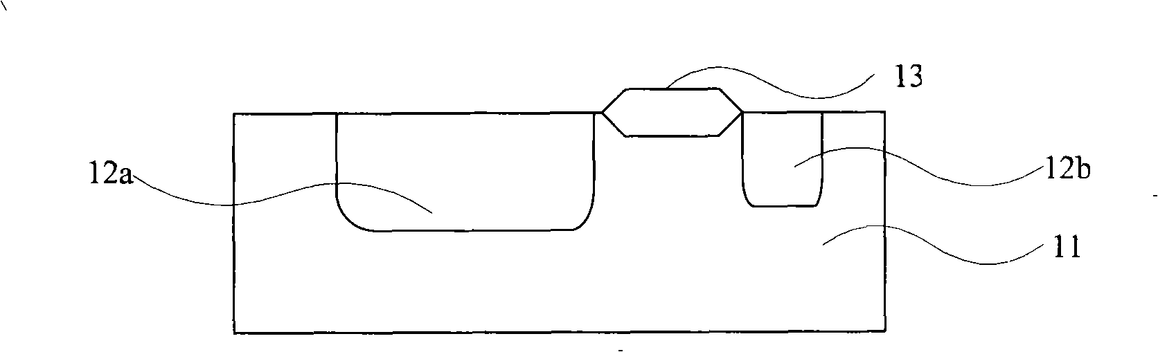
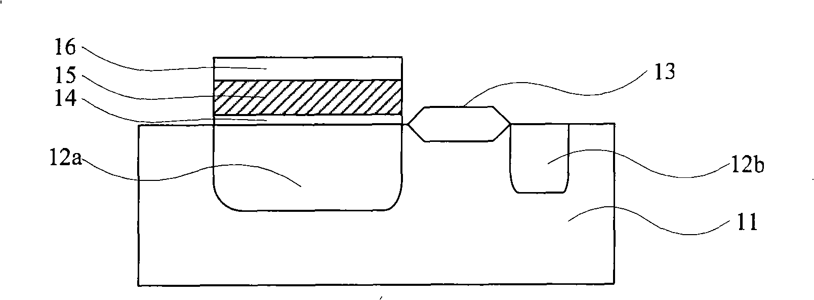
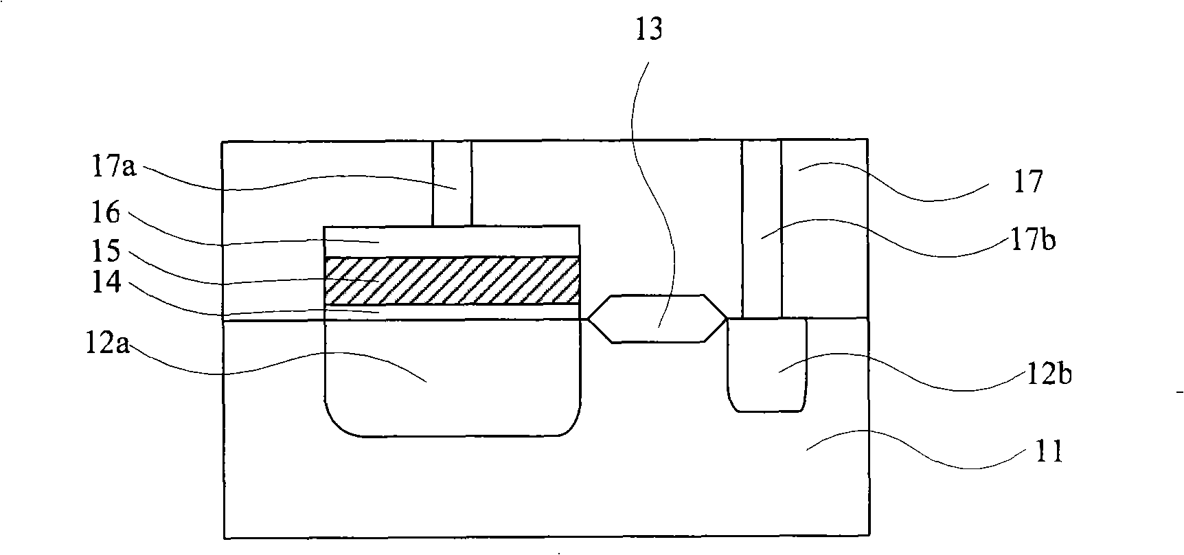
[0027] The essence of the present invention is to provide a test structure for the integrity of the gate dielectric layer and its formation method. The present invention forms the integrity of the gate dielectric layer of the present invention by forming isolation grooves, gate dielectric layers, and gate electrode layers on the semiconductor substrate. Sexual test structure. Apply a negative gate voltage on the gate electrode through the probe, ground the semiconductor substrate, and conduct an electrical test. Since the contact resistance between the probe and the gate electrode is small, the electrical test result is consistent with the integrity of the gate dielectric layer in the prior art. The test results of the test structure are comparable, and the repeatability of the test results is good, indicating that the test result of the test structure using the integrity of the gate dielectric layer of the present invention is reliable and can accurately reflect the integrity ...


PUM


Abstract

A forming method of a grid dielectric layer integrality test structure includes: forming an insulated groove in a semiconductor substrate as active region insulation; sequentially forming a dielectric layer, a multi-crystal silicon layer and an electrode layer on the semiconductor substrate; etching the dielectric layer, the multi-crystal silicon layer and the electrode layer to sequentially form a grid dielectric layer, a grid multi-crystal silicon layer and a grid electrode layer. Accordingly, the invention provides a test structure and a test method for grid dielectric layer integrality. The grid dielectric layer integrality test structure is formed by two layers of mask board and has analogous electricity test result to an existing grid dielectric layer integrality test structure formed by employing four layers of mask board, synchronously electricity test result repeatability of the grid dielectric layer integrality test structure of present invention is good, thereby saving technique cost, shortening technique circulation period and reducing technique risk.

Description

technical field [0001] The invention relates to the field of semiconductor technology, in particular to a test structure for the integrity of a gate dielectric layer, a forming method and a test method thereof. Background technique [0002] Since the gate dielectric layer plays an important role in the integrated circuit (IC), the control of the gate dielectric layer integrity (GOI) is very important in the IC manufacturing industry. There are many reports on how to prepare the gate dielectric layer in current patents. For example, the Chinese patent applications with application number 200510129150 and application number 200510081046 provide the process of how to prepare the gate dielectric layer, but do not disclose how to test the integrity of the gate dielectric layer. . The integrity of the gate dielectric layer includes indicators such as the insulation of the gate dielectric layer and the crystal quality of the gate dielectric layer. In the prior art, because the pr...

Claims


Application Information

Patent Timeline
Patent Type & Authority Applications(China)
IPC IPC(8): H01L23/544H01L21/02H01L21/66
Inventor 司马良陆肇勇黄柏喻林丰文
Owner SEMICON MFG INT (SHANGHAI) CORP
Why Eureka
Try Eureka