
Sputtering film forming method, electronic device manufacturing method, and sputtering system

A technology for sputtering thin films and sputtering systems, which is applied in the fields of semiconductor/solid-state device manufacturing, electrical components, semiconductor/solid-state device testing/measurement, etc. Design and control, improve efficiency, increase the effect of efficiency

Active Publication Date: 2010-06-09
CANON ANELVA CORP
View PDF5 Cites 0 Cited by
  • Summary
  • Abstract
  • Description
  • Claims
  • Application Information

AI Technical Summary

Problems solved by technology

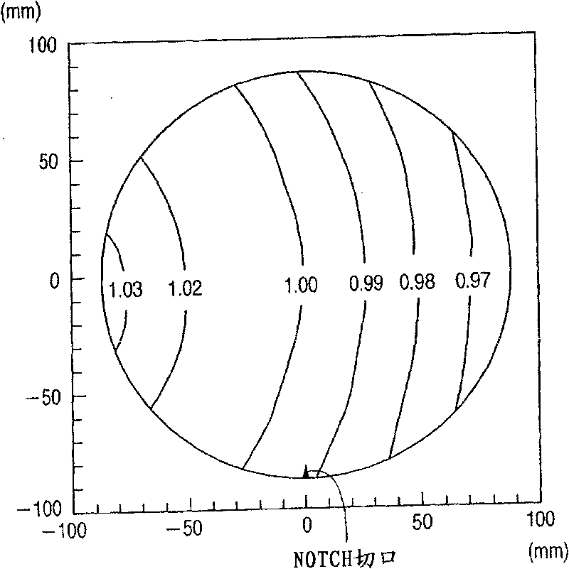
[0007] However, when such a film forming method is carried out, with respect to the film thickness distribution of each individual monolayer, the contour lines connecting positions with equal film thickness end to form arcs such as figure 2 , and it is difficult to obtain a film of a given film thickness including tilts in only a single direction
Therefore, when depositing a film including film thickness inclinations in two directions in the plane of the substrate, a satisfactory film thickness distribution cannot necessarily be obtained.
[0008] Therefore, it is assumed that the thickness control of the laminated film is insufficient in the case of, for example, the thin film manufacturing technology of the laminated film of the multi-nm order such as a metal / high-k gate stack, and the thickness of the multiple laminated film appears to be inaccurate.
As a result, operations to determine stack configurations, which are necessary for high-precision design and control, are hindered

Method used


Image

  • Sputtering film forming method, electronic device manufacturing method, and sputtering system
  • Sputtering film forming method, electronic device manufacturing method, and sputtering system
  • Sputtering film forming method, electronic device manufacturing method, and sputtering system

Examples


no. 1 approach

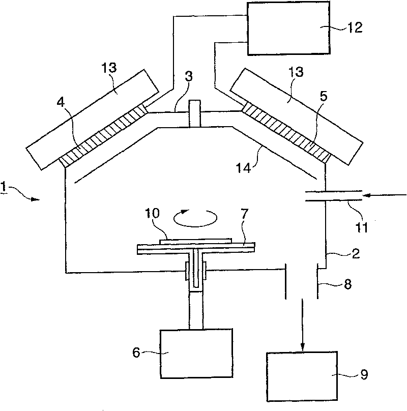
[0046] Figure 4 The sputtering system depicted in is used to form a single-layer hafnium film.

[0047] As the substrate 10, A silicon (Si) wafer is placed on the substrate holder 7, and the atmospheric pressure of the vacuum container 2 is reduced to 0.02 Pa. The baffle mechanism 14 is used to select a hafnium target, argon (Ar) gas is supplied as a discharge gas to the vacuum vessel 2 at 44.6 mg / min, and sputtering is performed.

[0048] In this case, a cut is made in the edge portion of the wafer as the sputtering start point, and the sputtering starts when the cut passes a predetermined position as the start point, and when the cut passes, rotates from the start point in the circumferential track direction Sputtering stops at the half-turn position. The rotation speed of the wafer is 2 rpm. Assuming that the power applied to the target is 100 watts, so that the thickness of the hafnium film at the center of the substrate 10 will be 10 nm.

[0049] The thickness distribution ...

no. 2 approach

[0051] Figure 4 The sputtering system depicted in is used to form a stacked film of hafnium and tantalum films.

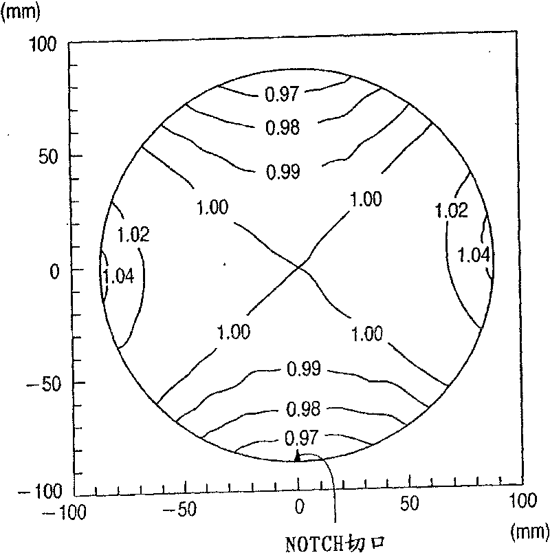
[0052] In order to deposit the thickest area of ​​the tantalum film on the thinnest area of ​​the hafnium film formed according to the first embodiment, establish the position of the notch on the wafer, use the baffle mechanism 14 to select the tantalum target, and the argon (Ar) gas at 44.6 mg / Provided separately, and perform sputtering. Assuming that the power applied to the target is 100 watts, so that the thickness of the tantalum film will be 10 nm at the center of the substrate 10. Thus, a laminated film in which a tantalum film is laminated on a hafnium film is obtained.

[0053] The thickness distribution of the laminated film thus obtained was measured using an ellipsometer, and the results are shown in Image 6 Portrayed in. Although the hafnium film and the tantalum film are laminated in such a manner that the film thickness is inclined by a given value, ...

no. 3 approach

[0058] The following is a description of electronic devices applicable to the present invention with reference to the accompanying drawings.

[0059] Figure 7 It is a flowchart depicting the electronic device manufacturing method according to the third embodiment. Figure 8 It is a conceptual configuration diagram depicting the MOS transistor 77 used according to the third embodiment. Picture 9 It is a conceptual configuration diagram of the MOS transistor 77 used in each respective manufacturing process according to the third embodiment.

[0060] In order to make Figure 8 The contact resistance between the gate electrode 73 of the MOS transistor depicted in and the wire 71 to the gate electrode is minimized, and it is necessary to install a compound 75 of nickel, platinum, and silicon (hereinafter referred to as "nickel platinum film 75"). Assuming that regarding the double-layer film of nickel and platinum formed on the MOS transistor 77, that is, the nickel-platinum film 72, t...


PUM

PropertyMeasurementUnit
thicknessaaaaaaaaaa
thicknessaaaaaaaaaa

Abstract

A sputtering film forming method. which positions a target 4 and 5 at an incline to a surface of a substrate 10 whereupon a film is to be formed, and forms the film upon the surface of the substrate 10 whereupon the film is to be formed in an incline direction while the substrate 10 is rotated about a normal axis, terminates the forming of the film at a predetermined timing from the commencement of the forming of the film, wherein the forming of the film is terminated, when the substrate has rotated by 360 degreesxn+180 degrees+alpha, where n is a natural number, including 0, and -10 degrees<alpha<10 degrees.

Description

Technical field [0001] The present invention relates to a sputtering film forming method for forming a thin film, an electronic device manufacturing method, and a sputtering system, for example, a semiconductor device manufacturing process. Background technique [0002] The development of semiconductor ultra-miniaturization technology is currently being carried out at a violent speed in order to use LSI to achieve greater speed and lower power consumption. Regarding a conventional transistor, a silicon nitride film is used as its gate insulator film, and a polysilicon film is used as its electrode. The silicide, which is a compound produced by silicon and metal, is used to reduce the resistance of the diffusion layer and reduce the contact resistance. [0003] However, recently, research on transistor technology is underway, which combines a metal gate electrode and a high-k gate dielectric film in order to maintain the decrease in current driving force due to the increased thickn...

Claims


Application Information

Patent Timeline
Patent Type & Authority Patents(China)
IPC IPC(8): H01L21/02H01L21/66H01L21/00C23C14/34
Inventor 北野尚武山田直树角田隆明山口述夫小须田求
Owner CANON ANELVA CORP
Learn More