
Method for preparing SON type metal oxide semiconductor field effect pipe device

A technology of oxide semiconductors and field effect transistors, which is applied in semiconductor/solid-state device manufacturing, electrical components, circuits, etc., can solve problems such as the inability to truly apply VLSI manufacturing processes, high price and cost, and reduced production efficiency. Facilitate industrial production of large-scale integrated circuits, reduce production costs, and achieve low cost

Active Publication Date: 2008-11-05
汉摩尼(江苏)光电科技有限公司
View PDF0 Cites 5 Cited by
  • Summary
  • Abstract
  • Description
  • Claims
  • Application Information

AI Technical Summary

Problems solved by technology

However, low-energy ion implantation will increase the divergence of ion beams and reduce production efficiency, so low-energy ion implantation has become a problem; at the same time, helium (He) and hydrogen (H) are both very light ions, and the range of ion implantation is relatively long. Difficult to control and get super shallow knot depth
In addition, implanting single crystal silicon (Si) with helium (He) to form a cavity must use a very high dose (usually greater than 10 16 cm -2 ), and helium (He) gas is a scarce resource in China, and its price is relatively high
Therefore, the above-mentioned prior art cannot really be applied to the current VLSI manufacturing process.

Method used


Image

  • Method for preparing SON type metal oxide semiconductor field effect pipe device
  • Method for preparing SON type metal oxide semiconductor field effect pipe device
  • Method for preparing SON type metal oxide semiconductor field effect pipe device

Examples


Embodiment Construction

[0036] Preferred embodiments of the present invention are described in detail below.

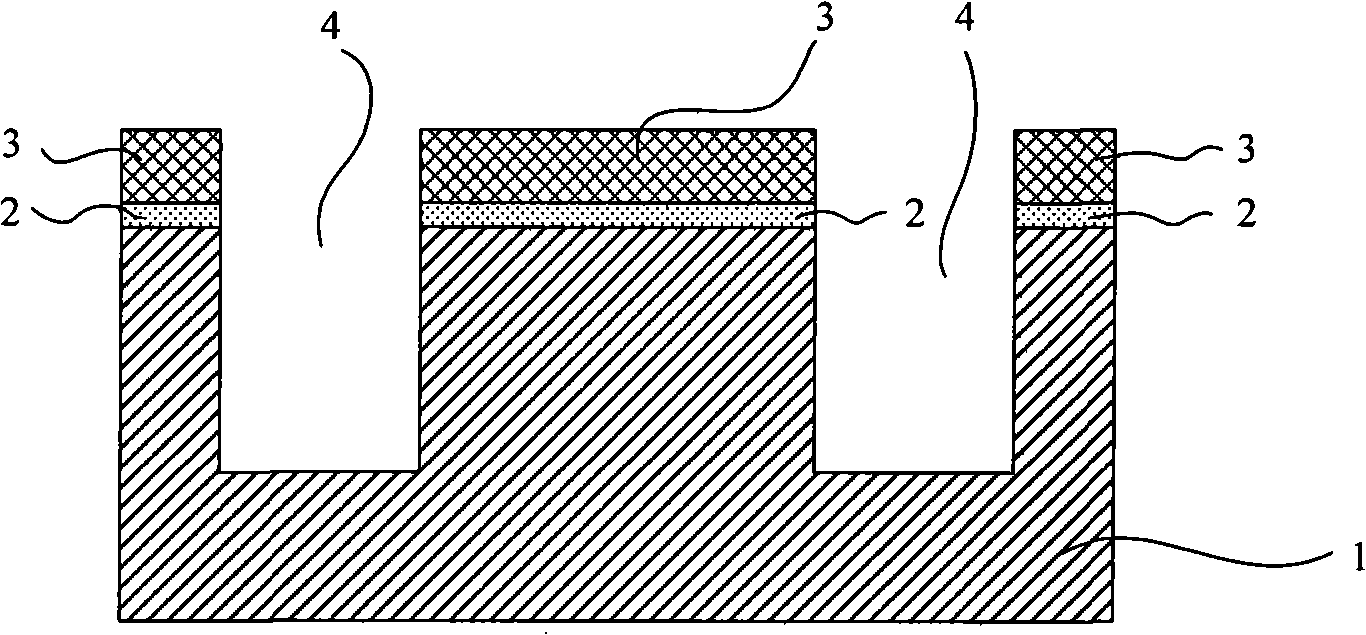
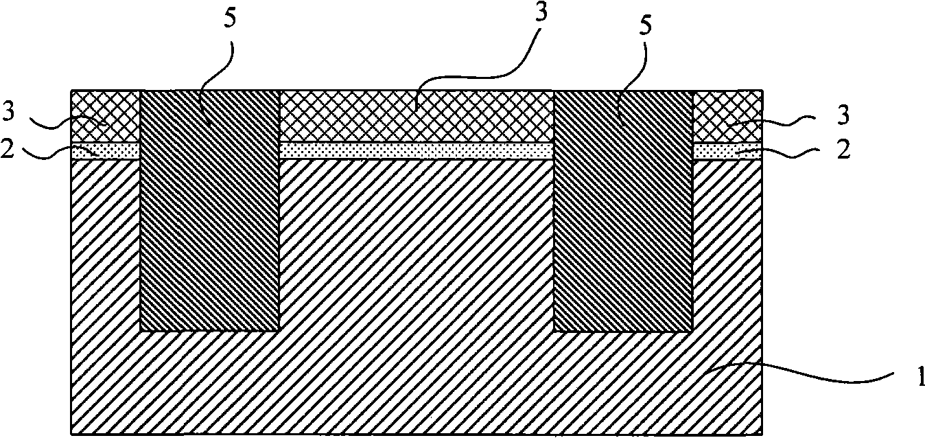
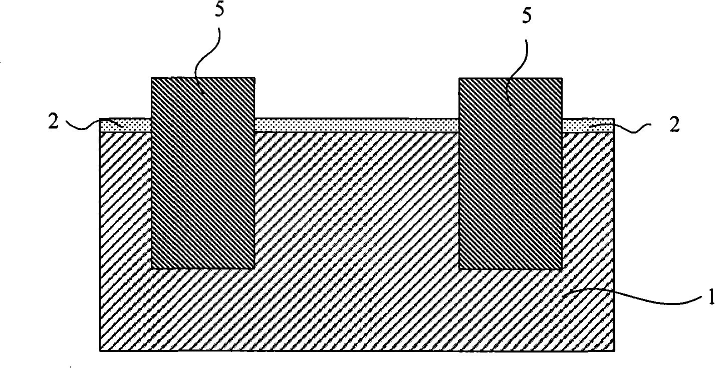
[0037] In the preparation method of the SON (Silicon-On-Nothing) type metal-oxide-semiconductor field effect transistor (MOSFET) device of the present invention, high insulation is obtained due to the technology of using low-cost neon ions implanted twice with different energies to form holes. The hollow layer with high performance has heat dissipation channels in the silicon substrate, thereby improving the defects of the SON device structure. At the same time, it is fully compatible with the conventional CMOS process, the process is simple, it is convenient for large-scale integrated circuit industrial production, and the production cost is reduced.

[0038] In the preparation method of the SON type metal oxide semiconductor field effect transistor device of the present invention, because the performance of forming the cavity layer in the gas ion implantation silicon chip depends on the bub...


PUM


Abstract

The invention discloses a preparation method of the SON type metal-oxide semiconductor field transistor, including the steps of low temperature injecting the neon ion with secondary different energy in the large beam current, forming the void layer at the lower part of the active region after high temperature anneal; removing the silicon nitride side wall on the shallow trough insulation, preparing the MOSFET through the routine CMOS technology. The preparation method providing the SON type metal-oxide semiconductor field transistor can generate the air bubble with higher density due to the low dose Ne iron injection, adopts the low temperature with different energy to form two layers of air bubble belts, which combines to be the high relative density monolayer inanition after high temperature anneal, thereby forming the ultra-shallow junction SON structure with the heat emission channel with simple technology and low cost. Most steps are completed by the routine CMOS technology, which is convenient for the large scale integrated circuit industrial production and reduced in the production cost.

Description

technical field [0001] The invention relates to the technical field of VLSI manufacturing, in particular to a method for preparing a SON (Silicon-On-Nothing) metal-oxide-semiconductor field effect transistor (MOSFET) device with silicon as a heat dissipation channel. Background technique [0002] In order to improve the performance and performance-price ratio of integrated circuit chips, it is a main way to reduce the feature size of the device to increase the integration level. However, as the size of the device shrinks, power consumption and leakage current become the most concerned issues. Silicon-On-Insulator SOI (Silicon-On-Insulator) structure has become the preferred structure of deep submicron MOS devices because it can well suppress the short channel effect and improve the ability of devices to be scaled down. [0003] Along with the continuous development of SOI technology, the 2179th page of electronic device volume 147, 2000, the 11th phase in prior art literatu...

Claims


Application Information

Patent Timeline
Patent Type & Authority Applications(China)
IPC IPC(8): H01L21/336
Inventor 彭本贤俞挺于峰崎
Owner 汉摩尼(江苏)光电科技有限公司
Learn More