Process for synthesizing high molecular nanometer composite material with pressure-sensitive performance and use

A nano-composite material and synthesis process technology, applied in the field of polymer nano-composite materials, can solve the problems of high additional capacitance, less impact resistance, short life, etc., and achieve the effect of highly reliable product performance and efficient production.

Inactive Publication Date: 2008-11-26
上海思麦电子有限公司
View PDF1 Cites 12 Cited by
  • Summary
  • Abstract
  • Description
  • Claims
  • Application Information

AI Technical Summary

Problems solved by technology

[0002] At present, there are mainly three types of components used for overvoltage protection of electronic circuits: ceramic varistors, silicon-based semiconductor transient overvoltage protection components and polymer ESD protection components: ceramic varistors are doped with ceramics, at high temperatures Bottom sintering semiconducting, made of roasted electrodes at both ends, its main disadvantages are high energy consumption, short life, less impact resistance, and poor pressure-sensitive

Method used


Image

  • Process for synthesizing high molecular nanometer composite material with pressure-sensitive performance and use

Examples


Embodiment 1

[0019] Metal nanomaterials and semiconductor ceramic nanomaterials are uniformly blended with polymer matrix materials to make homogeneous polymer nanocomposites, and the weight percent of each component is:

[0020] Metal nanomaterials Nickel (particle size 150nm) 23%

[0021] Semiconductor ceramic nanomaterials Zinc oxide (particle size 120nm) 12%

[0022] Polymer matrix material Epoxy resin 65%

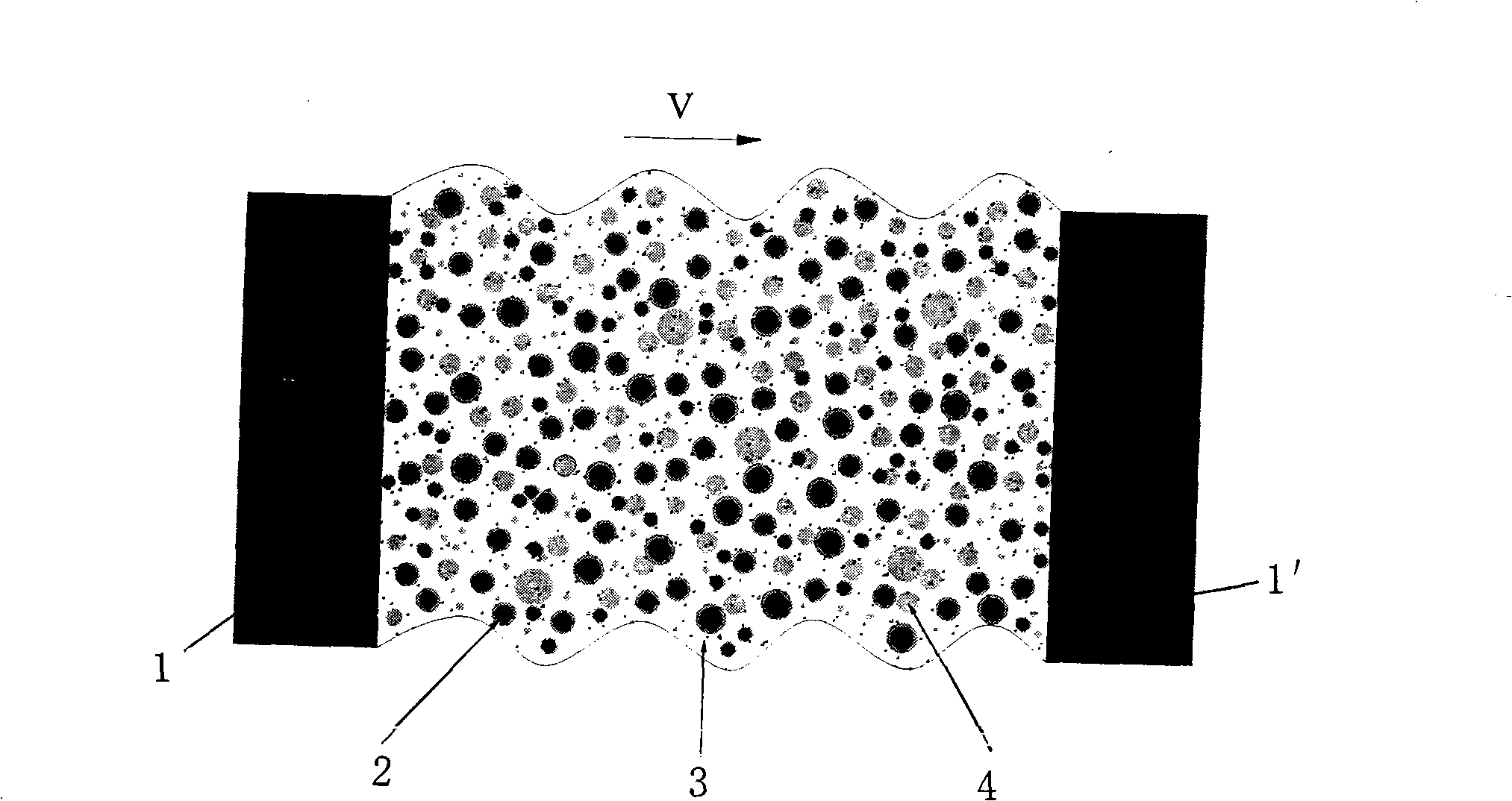
[0023] Add about 5% curing agent T31 of the total weight in the above-mentioned composite material slurry, stir for more than 5 hours, stop stirring after its viscosity gradually increases, put it into a container for use, and use it to make polymer nanocomposite materials. Sensitive components. Use the method disclosed in Chinese Patent Application No. 200810032677.8 to print it on the etched PCB board, and heat it to cure it. Press the printed circuit board on a PCB board with etched graphics, and make graphics on the entire board after compounding, lead the electrodes of the ...

Embodiment 2

[0027] Operate in the same manner as in Example 1, and each component and percentage by weight thereof are changed into:

[0028] Metal nanomaterials nickel + copper (both particle sizes are 120nm) 25%

[0029] Semiconductor ceramic nanomaterials Zinc oxide + silicon carbide (particle size 100nm) 20%

[0030] Polymer matrix material Epoxy resin 55%

[0031] The prepared nano-polymer composite slurry is used to make polymer nano-composite pressure-sensitive elements, the distance between electrodes is 0.1mm, the pressure-sensitive breakdown voltage Vbr is 200V, and the pressure-sensitive clamping voltage Vc is 45V.

Embodiment 3

[0033] Operate in the same manner as in Example 1, and each component and percentage by weight thereof are changed into:

[0034] Metal nanomaterials Nickel (particle size 120nm) 35%

[0035] Semiconductor ceramic nanomaterials Zinc oxide (particle size 100nm) 20%

[0036] Polymer matrix material Silicone resin 45%

[0037] The prepared nano-polymer composite slurry is used to make polymer nano-composite pressure-sensitive elements, the distance between electrodes is 0.05mm, the pressure-sensitive breakdown voltage Vbr is 300V, and the pressure-sensitive clamping voltage Vc is 80V.


PUM

PropertyMeasurementUnit
Particle sizeaaaaaaaaaa

Abstract

The invention relates to a synthetic technology for a macromolecular nano-composite with pressure-sensitive characteristic, which is used for preparing a pressure-sensitive element with high performance and high precision. The materials with the following weight percent are uniformly mixed to prepare the uniform macromolecular nano-composite: 20 percent to 40 percent of metal nanometer material, 10 percent to 30 percent of semiconductor ceramic nanometer material and 40 percent to 70 percent of macromolecular base material; wherein, the grain diameter of the metal nanometer material and the semiconductor ceramic nanometer material is 10nm to 500nm. The synthetic technology has the positive effect that metal nanometer powder and semi-conducting ceramic nanometer powder are fully mixed with the macromolecular material to form uniform homogeneous phrase, and the surface effect and the quantum size effect of the nanometer material are used for forming macroscopical pressure-sensitive effect. The technology for combining the macromolecular nano-composite, a circuit board and a semiconductor can efficiently produce various pressure-sensitive units; the performance of the product is highly reliable and the production cost is only a fraction of the traditional method.

Description

technical field [0001] The invention relates to a polymer nanocomposite material with pressure-sensitive properties and its application in the manufacture of pressure-sensitive elements. Background technique [0002] At present, there are mainly three types of components used for overvoltage protection of electronic circuits: ceramic varistors, silicon-based semiconductor transient overvoltage protection components and polymer ESD protection components: ceramic varistors are doped with ceramics, at high temperatures Bottom sintering semiconducting, made of roasted electrodes at both ends, its main disadvantages are high energy consumption, short life, less impact resistance, and poor pressure-sensitive characteristics; silicon-based semiconductor transient overvoltage protection components use semiconductor Its main features are large product investment, high production cost, large environmental pollution, and high additional capacitance of the product; polymer ESD protectio...

Claims


Application Information

Patent Timeline
IPC IPC(8): C08L63/00C08L83/00C08L33/00C08K3/08C08K3/22C08K3/14
Inventor 张建
Owner 上海思麦电子有限公司
Why Eureka
Try Eureka