Semiconductor nanocrystalline and method for preparing same

A nanocrystal and semiconductor technology, applied in the field of nanomaterials, can solve the problems of difficult to find synthesis conditions, difficult to obtain semiconductor nanocrystals, unstable, etc., and achieve the effects of controllable morphology, moderate reaction conditions and low cost.

Active Publication Date: 2008-11-26
JIANGSU LIANGDIAN TECH CO LTD
View PDF0 Cites 10 Cited by
  • Summary
  • Abstract
  • Description
  • Claims
  • Application Information

AI Technical Summary

Problems solved by technology

[0004] At present, the synthesis technology of nanocrystals such as CdSe and CdTe has been relatively mature, and the size and shape have been well controlled, but the synthesis of nanocrystals of some materials is still There are many problems. For example, mercury compounds are usually extremely unstable in the organic phase at a temperature greater than 100 degrees. It is difficult to find controllable synthesis conditions. At the same time, it has controllable shape and size, high luminous efficiency, and adjustable luminous range. Semiconductor nanocrystals are also difficult to obtain

Method used


Image

  • Semiconductor nanocrystalline and method for preparing same
  • Semiconductor nanocrystalline and method for preparing same
  • Semiconductor nanocrystalline and method for preparing same

Examples


Embodiment 1

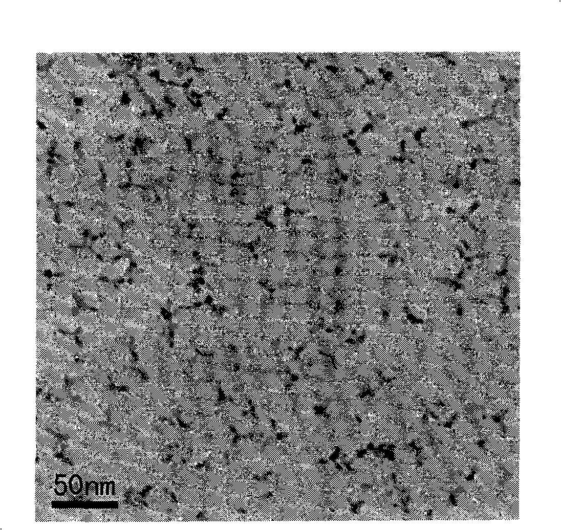
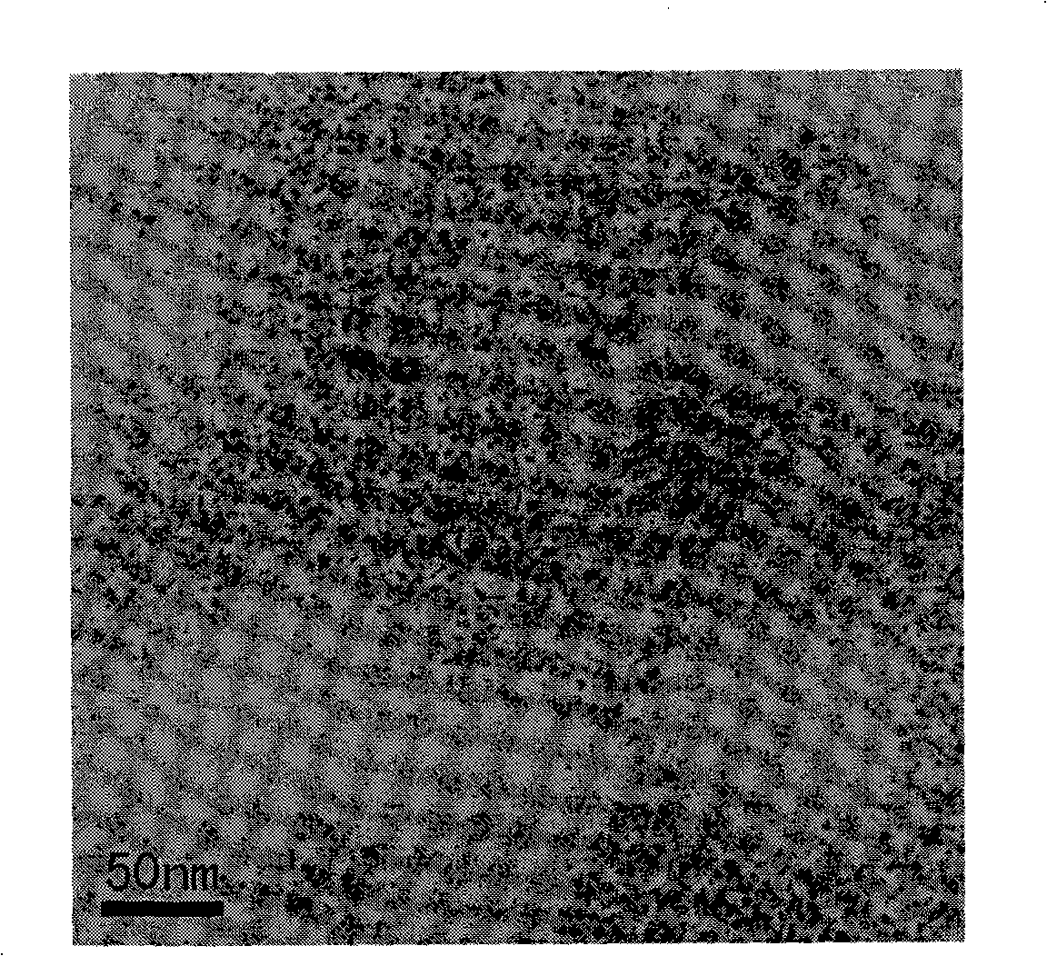
[0027] The preparation concentration is 1.3×10 -2 mol / L CdTe toluene solution, take 2.1ml of this solution, add 0.2ml dodecylmercaptan while stirring at room temperature, and then add 0.02ml 0.335mol / L Hg(ClO 4 )·3H 2 O methanolic solution, stirred for 10 min until the solution turned from dark red to brown to give branched Hg 0.2 Cd 0.8 Te nanocrystals. The transmission electron microscope pictures of CdTe nanocrystals are shown in figure 1 , the resulting Hg 0.2 Cd 0.8 The electron microscope transmission photo of Te nanocrystals is shown in figure 2 , UV-Vis absorption spectrum see Figure 6 , the fluorescence absorption spectrum see Figure 7 .

Embodiment 2-4

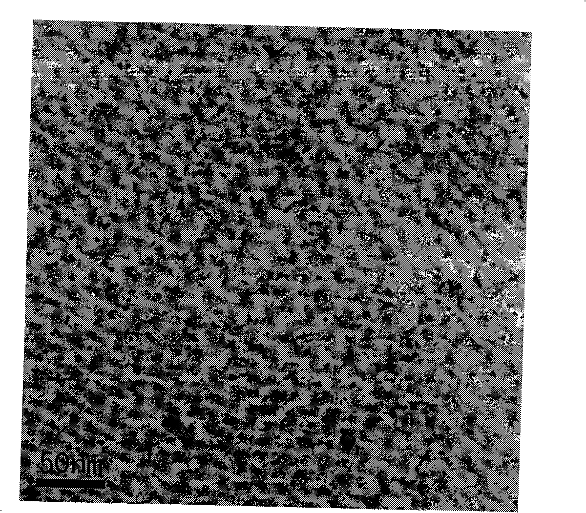
[0029] Add Hg(ClO 4 )·3H 2 The amount of O methanol solution is respectively 0.027ml, 0.04ml and 0.06ml, and other is with embodiment 1, obtains branched semiconductor nanocrystal Hg respectively after stirring 0.25 Cd 0.75 Te, Hg 0.33 Cd 0.67 Te and Hg 0.43 Cd 0.57 Te, see TEM pictures respectively image 3 , Figure 4 , Figure 5 , UV-Vis absorption spectrum see Figure 6 , the fluorescence absorption spectrum see Figure 7 .

Embodiment 5

[0031] The preparation concentration is 5.2×10 -3 mol / L ZnSe toluene solution 4ml, under nitrogen protection, add 0.018ml dodecyl mercaptan under stirring, heat to 60°C, inject 0.9mL cadmium nitrate solution with a concentration of 0.1M in three times of 0.3ml, At 6 minutes, the temperature was raised to 100 degrees and kept at this temperature, samples were taken and measured at 8 minutes and 18 minutes respectively, and the fluorescence spectrum curves were shown in Figure 8 For a and b, inject 0.3mL cadmium nitrate solution at 45 minutes, and continue to react for 18 minutes and 30 minutes to take samples for measurement. The fluorescence spectra are shown in Figure 8 Curves c and d. In this example, the spectra of semiconductor nanocrystals obtained by adding excess reactants are measured as a function of time.


PUM

PropertyMeasurementUnit
sizeaaaaaaaaaa

Abstract

The invention relates to a semiconductor nano-crystal and a preparation method thereof. The composition of the semiconductor nano-crystal is as follows: AXB1-XC with x bigger than 0 and smaller than 1; wherein A is Cd or Zn: when A is Cd, B is Hg and C is Te; when A is Zn, B is Cd or Cu and C is Se. During preparation, the CdTe or ZnSe nano-crystal is firstly dissolved in reaction solvent with mercaptan of C4 to C12 as a stabilizer, and then reacts with the solution acquired by dissolving mercury salt, cadmium salt or copper salt in organic solvent while the temperature remains 20 to 100 DEG C, and the semiconductor nano-crystal AXB1-XC is got. The semiconductor nano-crystal prepared by the method has a controllable size, shape and appearance, a high luminous efficiency, and a luminous range which can be adjusted as required. The preparation method has the advantages of simplicity, controllable condition, placid reaction condition and low cost and the preparation method is worth promoting.

Description

(1) Technical field [0001] The invention relates to a semiconductor nanocrystal and a preparation method thereof, belonging to the technical field of nanomaterials. (2) Background technology [0002] In recent years, the application of far-infrared and near-infrared luminescent nanocrystals in biological detection has aroused the research interest of many workers. These nanocrystals can effectively weaken the influence of autofluorescence on detection signals, and their excitation wavelength and emission The wavelength is not absorbed by interstitial fluids such as water and hemoglobin. Therefore, nanocrystals with infrared detection ability have a good application prospect in biological detection. [0003] Around how to use near-infrared luminescent nanocrystals as imaging units in the biological field, there are currently two main problems. First, the synthesis technology of near-infrared nanocrystals is not well established; secondly, the toxicity and instability of nea...

Claims


Application Information

Patent Timeline
Patent Type & Authority Applications(China)
IPC IPC(8): C30B29/46C30B29/48
Inventor 李林松娄世云牛金钟
Owner JIANGSU LIANGDIAN TECH CO LTD
Why Eureka
Try Eureka