CMOS image sensor chip scale package with die receiving opening and method of the same

A technology of image sensors and grains, which is applied in semiconductor/solid-state device manufacturing, electric solid-state devices, semiconductor devices, etc., and can solve problems such as increased thickness

Inactive Publication Date: 2008-12-03
ADVANCED CHIP ENG TECH
View PDF0 Cites 13 Cited by
  • Summary
  • Abstract
  • Description
  • Claims
  • Application Information

AI Technical Summary

Problems solved by technology

Therefore, the thickness of the package will increase

Method used


Image

  • CMOS image sensor chip scale package with die receiving opening and method of the same
  • CMOS image sensor chip scale package with die receiving opening and method of the same
  • CMOS image sensor chip scale package with die receiving opening and method of the same

Examples


Embodiment Construction

[0018] Certain similar embodiments of the invention will not be described in detail. However, it should be understood that all the preferred embodiments in the present invention are only used for illustration rather than limitation. Therefore, except for the preferred embodiments herein, the present invention can also be widely applied in other embodiments. The dimensions of different components are not particularly described, and the dimensions of certain related components are enlarged and meaningless parts are omitted to clearly describe and emphasize the content of the present invention.

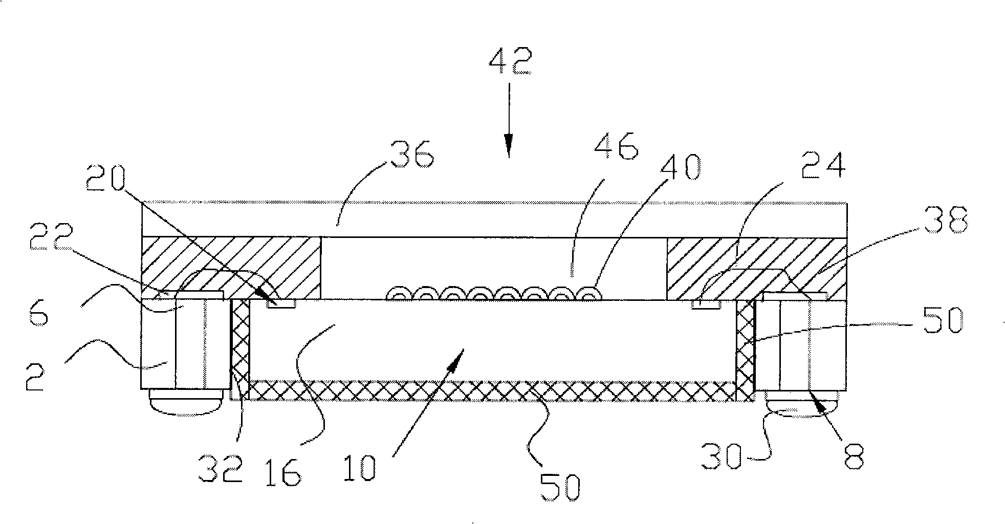
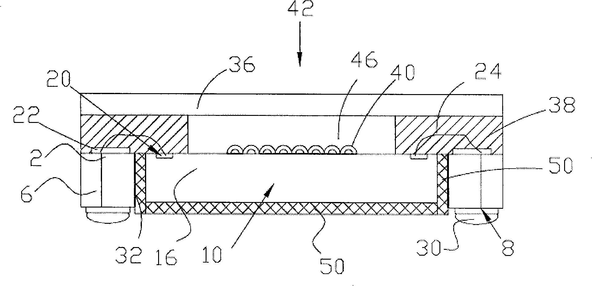
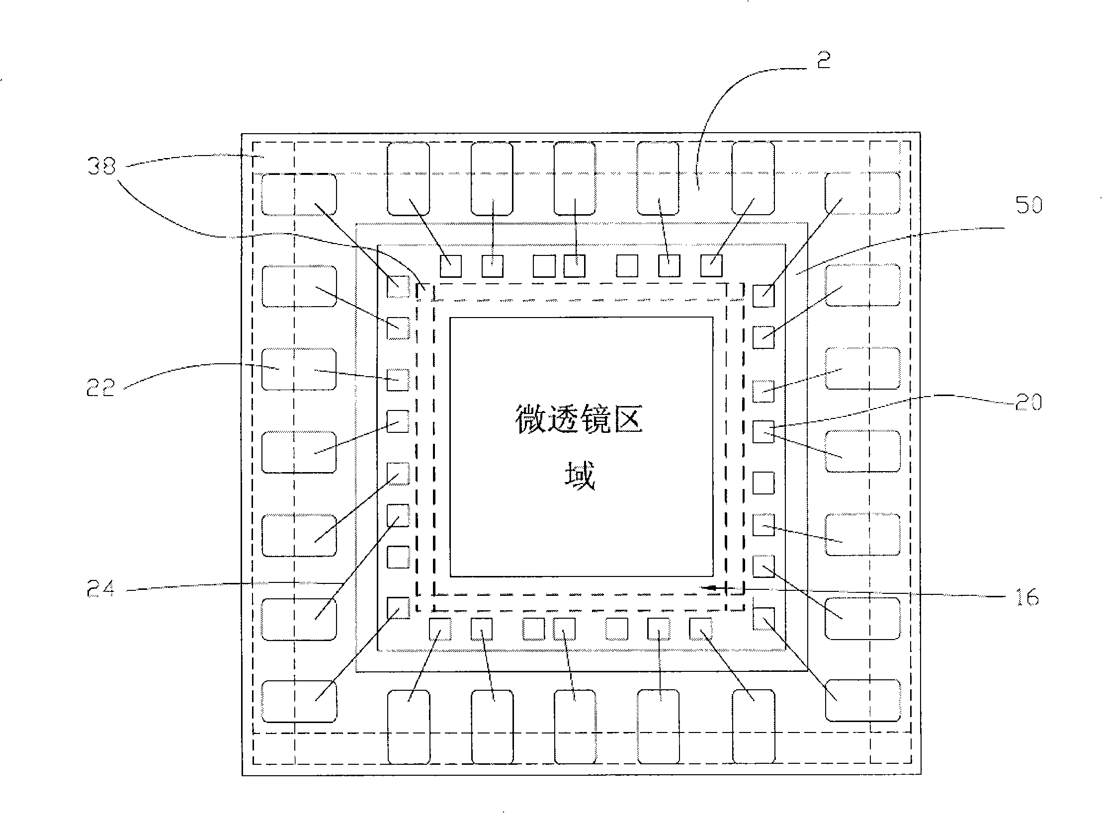
[0019] The invention discloses a PLP which adopts preset grain perforation and contact (internal connection) perforation on the substrate, the contact metal pad is located above the substrate, and the terminal contact pad is located below the substrate, and the two are connected through the metal in the perforation hole. A plurality of through holes pass through the substrate. Bonding w...


PUM

PropertyMeasurementUnit
thicknessaaaaaaaaaa

Abstract

The invention discloses a chip size image sensor with a grain receiving open and a manufacturing method thereof, comprising a grain receiving perforation and a substrate of the contact perforation, wherein a terminal contacting mat is formed below the contact perforation and above the substrate. The grain with a lens area is arranged in the grain receiving perforation through the adhesive paste materials. A thick dielectric layer is formed on the initiative surface of the grain and the upper surface of the substrate besides the microlens area. An output / input welding mat is formed on the grain and the substrate, for electrically connected the connecting wires coupled to a joining mat of the grain and the contact mat of the substrate. The core material is filled in the gap between the brim of the grain, the back of the grain and the side wall of the perforation. A transparent cover is arranged on the grain and the dielectric layer through the adhesive paste for generating a gap between the lens and the transparent cover. A conduction convex is selectively coupled to the terminal mat. The method and the method disclosed in the invention can be widely applied in the technical field of the semiconductor.

Description

technical field [0001] The present invention relates to a panel level package (panel level package, PLP), in particular to a substrate with a chip receiving opening for accommodating an image sensor chip. Background technique [0002] With the rapid development of semiconductor technology, it has become a trend to increase the density and miniaturization of semiconductor grains. Therefore, such high-density packaging technology and interconnection technology are also improved to apply the above-mentioned conditions. In the traditional flip chip structure, the array of solder balls is formed on the surface of the die, and the desired pattern is formed through the solder ball mask through the traditional solder paste. Packaging functions include heat dissipation, signal transmission, power distribution, protection, etc. When chips become more complex, traditional packaging such as lead frame packaging, flexible packaging, and rigid packaging cannot meet the needs of high-dens...

Claims


Application Information

Patent Timeline
Patent Type & Authority Applications(China)
IPC IPC(8): H01L27/146H01L23/488H01L21/50H01L21/60
CPCH01L24/85H01L2224/8592H01L2924/15153H01L2924/16235H01L2924/01004H01L24/48H01L27/14687H01L2924/01068H01L2924/09701H01L2224/48227H01L2924/14H01L2924/18165H01L27/14627H01L2224/48235H01L2924/01078H01L21/6835H01L2924/10253H01L27/14618H01L2224/48091H01L2224/49171H01L2924/3025H01L27/14683H01L24/97H01L2924/01077H01L2224/05554H01L2924/00014H01L24/49H01L2924/00H01L2224/45099H01L2224/45015H01L2924/207H01L27/14
Inventor 杨文焜张瑞贤许献文林殿方
Owner ADVANCED CHIP ENG TECH
Why Eureka
Try Eureka