Method for preparing polymer nanometer optical waveguide coupling beam divider

A production method and polymer technology, applied in the field of nanophotonics, can solve the problems of high cost, large size of the coupling part, complicated production method, etc., and achieve the effects of low cost, small optical loss, and good spectroscopic performance.

Inactive Publication Date: 2010-09-22
SUN YAT SEN UNIV
View PDF1 Cites 0 Cited by
  • Summary
  • Abstract
  • Description
  • Claims
  • Application Information

AI Technical Summary

Problems solved by technology

However, the size of the coupling part of the MMI-type optical beam splitter is relatively large, usually from hundreds to thousands of microns
In order to reduce the size of the device, submicron / nanoscale photonic crystals, plasmonic waveguides, and photonic wire waveguides have been introduced to separate / synthesize optical signals, but the fabrication methods are complex and expensive

Method used


Image

  • Method for preparing polymer nanometer optical waveguide coupling beam divider
  • Method for preparing polymer nanometer optical waveguide coupling beam divider
  • Method for preparing polymer nanometer optical waveguide coupling beam divider

Examples


Embodiment 1

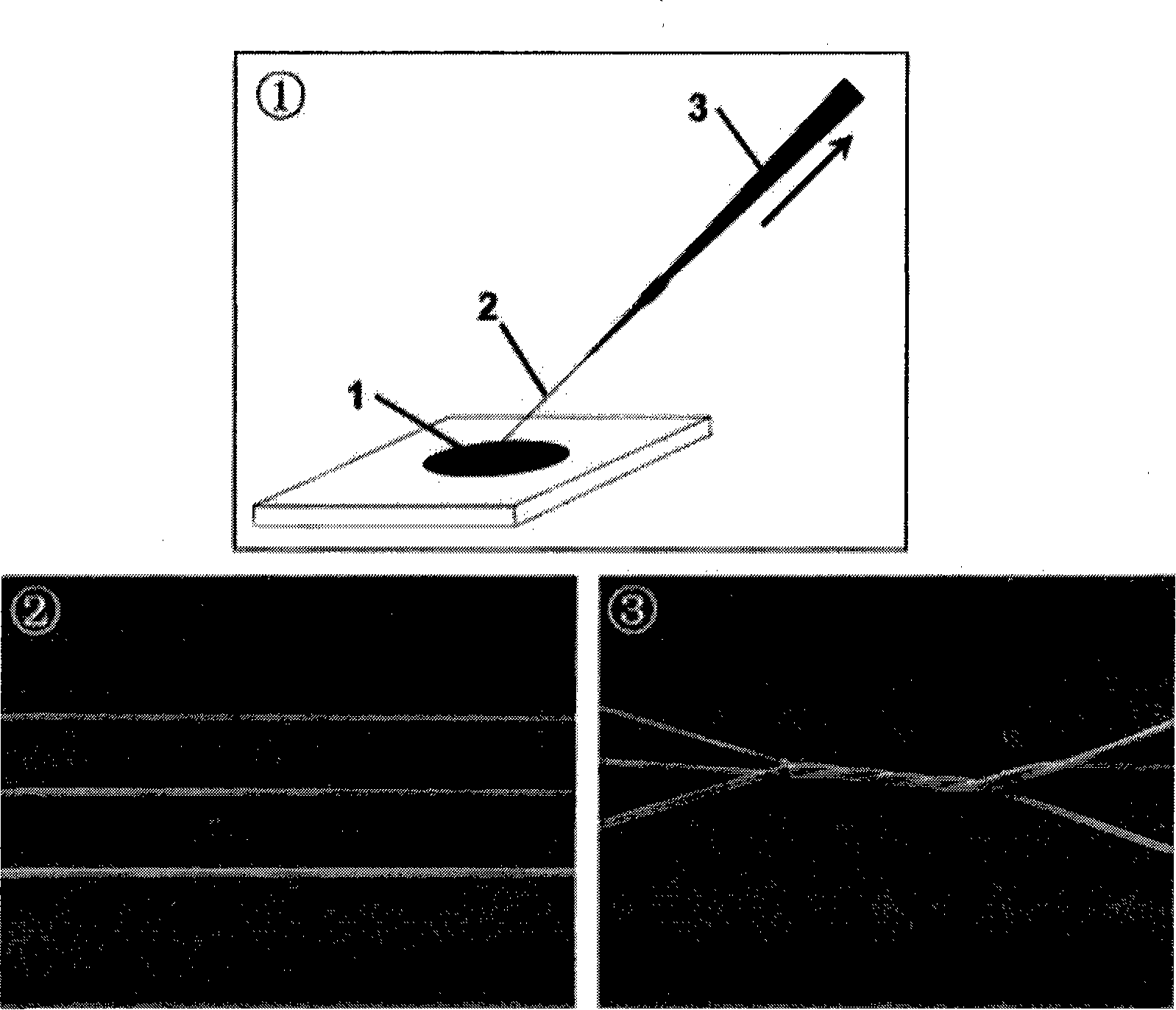
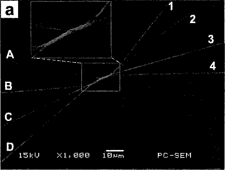
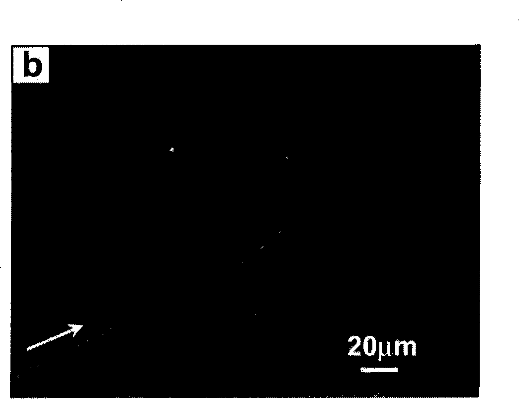
[0038] Four PTT nano-optical waveguides were wound and assembled to form a 4×4 optical power beam splitter using micro-operation winding technology, in which the diameters of the nano-optical waveguides from branch A to branch D were 450, 450, 510 and 570 nm, respectively. Figure 2(a) is the SEM image of the device. It can be seen from the inset that the device is composed of a 3×4 and 1×4 coupler cascaded, and the total width of the coupling part is 1.98 μm. The maximum length of the coupling part of the device is about 16.1 μm, and the coupling length of the 1×4 beam splitter is about 8.5 μm. The optical signal is coupled into the device by means of evanescent wave coupling, and then the optical splitting performance of the device is tested. Here the average value of the input and output total loss is 0.480dB. As shown in Figure 2(b), when the red light with a working wavelength of 650nm is coupled into branch B, it is divided into four parts and output from branches 1 to 4...

Embodiment 2

[0040] Figure 3 shows a 6×6 polymer nano-optical waveguide coupled beam splitter assembled by winding six PTT nano-optical waveguides. The diameters of the PTT fibers of branches A-F are 520, 540, 540, 540, 420, and 360 nm, respectively. The inset of Fig. 3(a) presents a magnified image of the winding part, where the coupling part has a length of 11–20 μm and a width of 2.92 μm. As shown in Figure 3(b), when the green light with a wavelength of 532nm is coupled into branch C, the coupled part is divided into six parts and output in branches 1-6, and the splitting ratio is 17:16:20:18:15: 14. In this case, the splitting uniformity of the beam splitter is 1.55dB. When blue light with a wavelength of 650nm is input into branch D, the power distribution of the six output branches of the beam splitter is very uniform, and the uniformity of light splitting is only 0.03dB ( Figure 3c ). Visible light of different wavelengths is also coupled into branches C and D, respectively, to d...

Embodiment 3

[0042] Figure 4 shows an 8×8 polymer nano-optical waveguide coupling beam splitter with a long coupling part, which is composed of 8 diameters of 400, 400, 400, 400, 400, 750, 750 and 600nm (branches A-H) The PTT nano-optical waveguide is assembled. As shown in the SEM image in the inset of Fig. 4(a), the length and width of the coupling part are approximately 38 μm and 2.5 μm. We coupled three kinds of visible light into 8×8 beam splitting to observe the splitting performance of the device. As shown in Figure 4(b), (c), red light and blue light are coupled into branches E and G respectively, and are divided into branches 1-8 for output through the coupling part.


PUM

PropertyMeasurementUnit
widthaaaaaaaaaa
lengthaaaaaaaaaa
widthaaaaaaaaaa

Abstract

The invention belongs to the field of nano-photonics, in particular to a production method of a polymer nano optical waveguide coupling beam splitter, which comprises the following steps: 1) the tip end of a SiO2 / metal rod (3) draws polymer nano optical waveguides (2) from polymer in the melting state or polymer solution (1) by using the drawing method; 2) the polymer nano optical waveguides (2) are parallelly arranged on a horizontal plane at equal intervals; and 3) an array of the parallel nano optical waveguides is rotated around a central horizontal shaft to form the polymer nano optical waveguide coupling beam splitter, the middle winding part thereof is a coupling region of optical signals, and a plurality of input and output branches are arranged on the both sides. The method of the invention has the advantages of simpleness, rapidness and low cost.

Description

technical field [0001] The invention belongs to the field of nanophotonics, in particular to a manufacturing method of a polymer nanometer optical waveguide coupling beam splitter. Background technique [0002] Ultra-compact photonic devices have broad application prospects in the fields of optical communication, sensing, and optical integration. Ultra-compact optical power beam splitters are important photonic devices for splitting / synthesizing optical signals, and play an important role in optical interconnection, integrated photonics, and biosensing. At present, micron-scale optical beam splitters have been realized on semiconductor materials (eg, InP, SOI, and SiGe / Si) using multi-step photolithography. However, since the bending radius of the micron-scale waveguide is too large, it does not allow a large number of 2×2 couplers or 1×2 beam splitters to be integrated on a substrate of several inches by cascading. To avoid the cascade approach, multimode interference (MM...

Claims


Application Information

Patent Timeline
Patent Type & Authority Patents(China)
IPC IPC(8): G02B6/28G02B1/04B29C55/00B29K67/00B29L11/00
Inventor 李宝军邢晓波朱恒王宇清张垚
Owner SUN YAT SEN UNIV
Why Eureka
Try Eureka