Eureka AIR delivers breakthrough ideas for toughest innovation challenges, trusted by R&D personnel around the world.

CMOS image sensor active pixel capable of changing operation mode and image sensor thereof

An image sensor and working mode technology, applied in the field of image sensors, can solve the problems of inability to eliminate reset noise, limitations, inability to adapt to high-speed image sensing, etc. Effect

Active Publication Date: 2008-12-24
TIANJIN HUIWEI ELECTRONICS RES & DEV SCI & TECH
View PDF0 Cites 15 Cited by
  • Summary
  • Abstract
  • Description
  • Claims
  • Application Information

AI Technical Summary

Problems solved by technology

Therefore, the full parallel exposure of four-tube pixels actually adopts the serial frame output method of "Sth frame exposure→Sth frame readout→S+1th frame exposure→S+1th frame readout", which cannot adapt to The need for high-speed image sensing up to 1,000 frames per second in monitoring and other fields
And because the T4 tube is shared by the whole frame, the reset signal located before the readout signal (Readout) cannot be output to the external double sampling circuit at one time. The reset signal obtained by the external double sampling circuit is actually specially designed for double sampling after the signal is read out. The reset signal generated by the reset operation has no time correlation with the readout signal, so the reset noise cannot be eliminated, which limits the application of this pixel structure in the field of large dynamic range.

Method used


Image

  • CMOS image sensor active pixel capable of changing operation mode and image sensor thereof
  • CMOS image sensor active pixel capable of changing operation mode and image sensor thereof
  • CMOS image sensor active pixel capable of changing operation mode and image sensor thereof

Examples


Embodiment Construction

[0037] The present invention will be described in detail below in conjunction with the accompanying drawings of the embodiments.

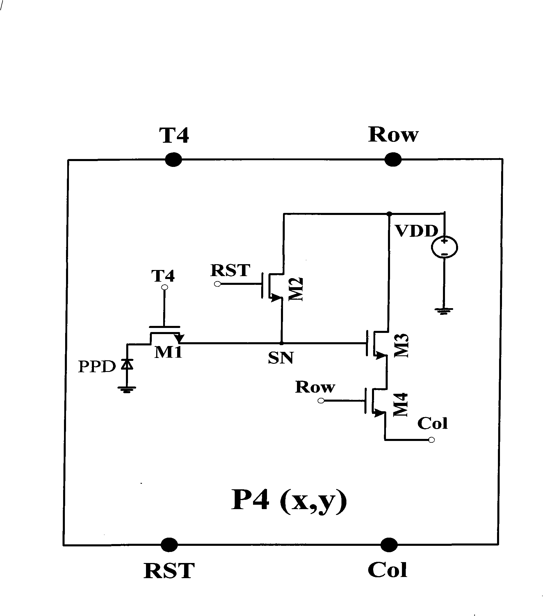
[0038] Such as Figure 7 As shown, the active pixel of the CMOS image sensor with changeable working mode of the present invention includes: a fifth MOS tube M5 for independent global exposure, a first MOS tube M1 for 4T / 5T transmission gate, and reset The second MOS tube M2, the third MOS tube M3 for buffering output and the fourth MOS tube M4 for row strobe are composed of the second MOS tube M2, the source of the first MOS tube M1 and the source of the second MOS tube M2 And the connection point of the gate of the third MOS transistor M3 is the storage node SN; the drain of the fifth MOS transistor M5, the drain of the second MOS transistor M2 and the drain of the third MOS transistor M3 are all connected The anode of the power supply; the source of the third MOS tube M3 is connected to the drain of the fourth MOS tube M4, the source of the fourth M...


PUM


Abstract

The invention relates to active pixels of a CMOS image sensor which can transform the working mode, and the image sensor thereof. Each active pixel comprises a first MOS tube source, a second MOS tube source and a third MOS tube gate; the connection points between the first and the second MOS tube sources and the third MOS tube gate are taken as storage nodes; a fifth MOS tube drain, a second MOS tube drain and a third MOS tube drain are connected with an anode of a power supply; a third MOS tube source is connected with a fourth MOS tube drain, a fourth MOS tube source is an output voltage signal, a fourth MOS tube gate is a line gating control line; a second MOS tube gate is a reset signal; a fifth MOS tube gate is a T5 gating signal, and a first MOS tube gate is a T4 gating signal. An exposure control module is respectively connected with the T4, the T5 gating signals and the reset signal of each active pixel; a line decoder is respectively connected with the line gating control line of each active pixel; a multiplexer is respectively connected with the output voltage signal of each active pixel; a 4T / 5T mode switching unit which is respectively connected with the exposure control module through 4T and 5T buses; and the 4T / 5T mode switching unit is connected with the multiplexer through the output data of the image sensor. The active pixels can greatly reduce the imaging noise under the dark light situation.

Description

Technical field [0001] The invention relates to an image sensor. In particular, it relates to a CMOS image sensor active pixel and its image sensor with a switchable working mode that can meet the practical application of the CMOS image sensor in the fields of high-speed monitoring, security protection and the like. Background technique [0002] The CMOS image sensor chip is a single-chip imaging system that collects image information through a large-scale two-dimensional photosensitive pixel array and converts its optical signals into corresponding analog or digital signals, which can realize high-speed and low-power electronic imaging functions . Among them, the CMOS active pixel as a photoelectric conversion unit occupies a core position in the entire CMOS image sensor architecture, and the quality of its structural design will directly affect the imaging performance of the CMOS image sensor. [0003] In practical applications in the fields of high-speed monitoring, security p...

Claims


Application Information

Patent Timeline
Patent Type & Authority Applications(China)
IPC IPC(8): H04N5/235H04N5/335H04N25/00
Inventor 李斌桥
Owner TIANJIN HUIWEI ELECTRONICS RES & DEV SCI & TECH
Why Eureka
Eureka Blog
Learn More