Method for enhancing dynamic range of quantum dot resonance tunneling diode photodetector
A technology of resonant tunneling and optical detectors, which is applied in the field of visible light and short-wave infrared detectors, and can solve the problem of small dynamic range of detectors
- Summary
- Abstract
- Description
- Claims
- Application Information
AI Technical Summary
Problems solved by technology
Method used
Image
Examples
Embodiment Construction
[0028] The working mode of the device will be further described below in conjunction with the accompanying drawings and implementation examples.
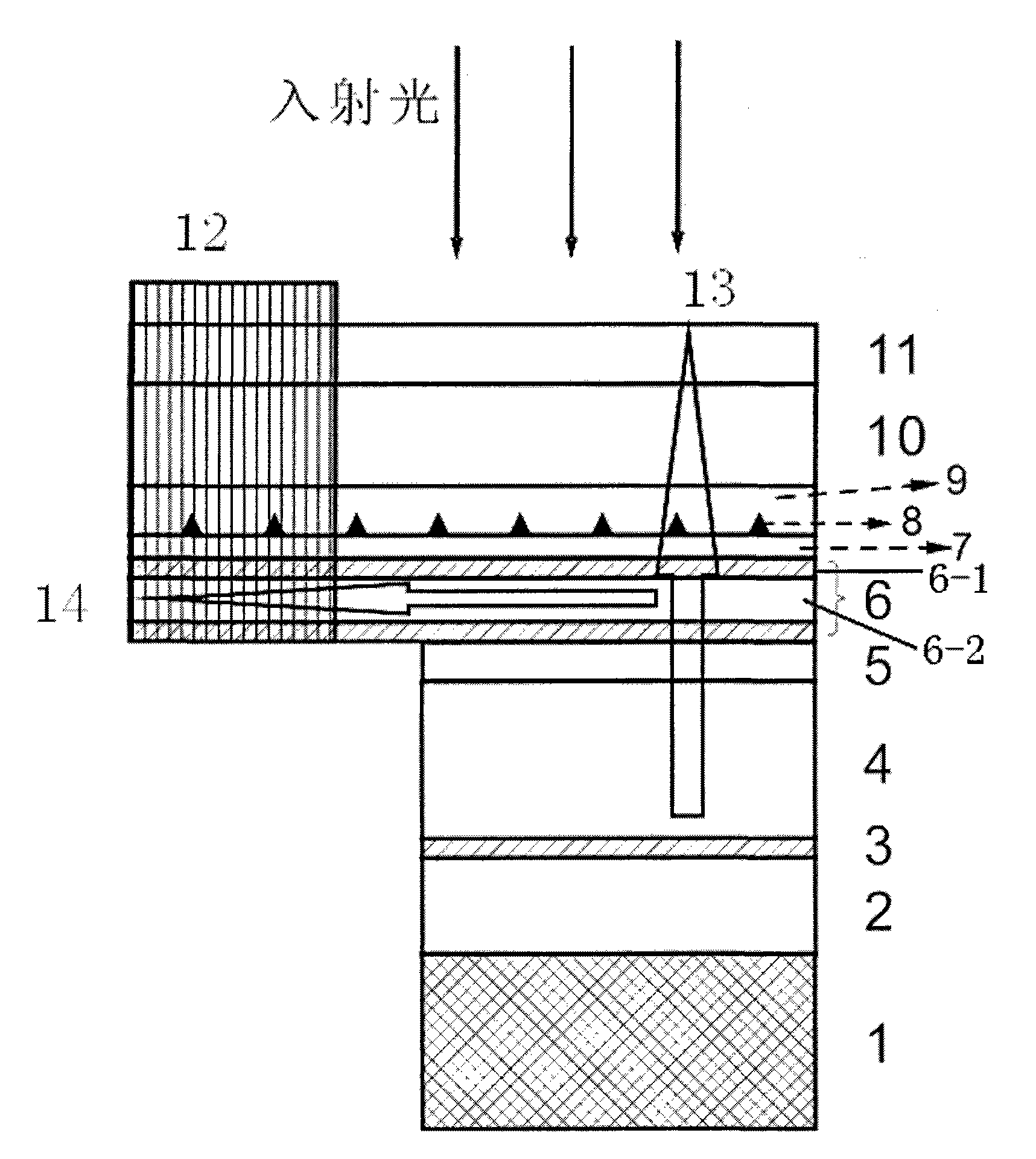
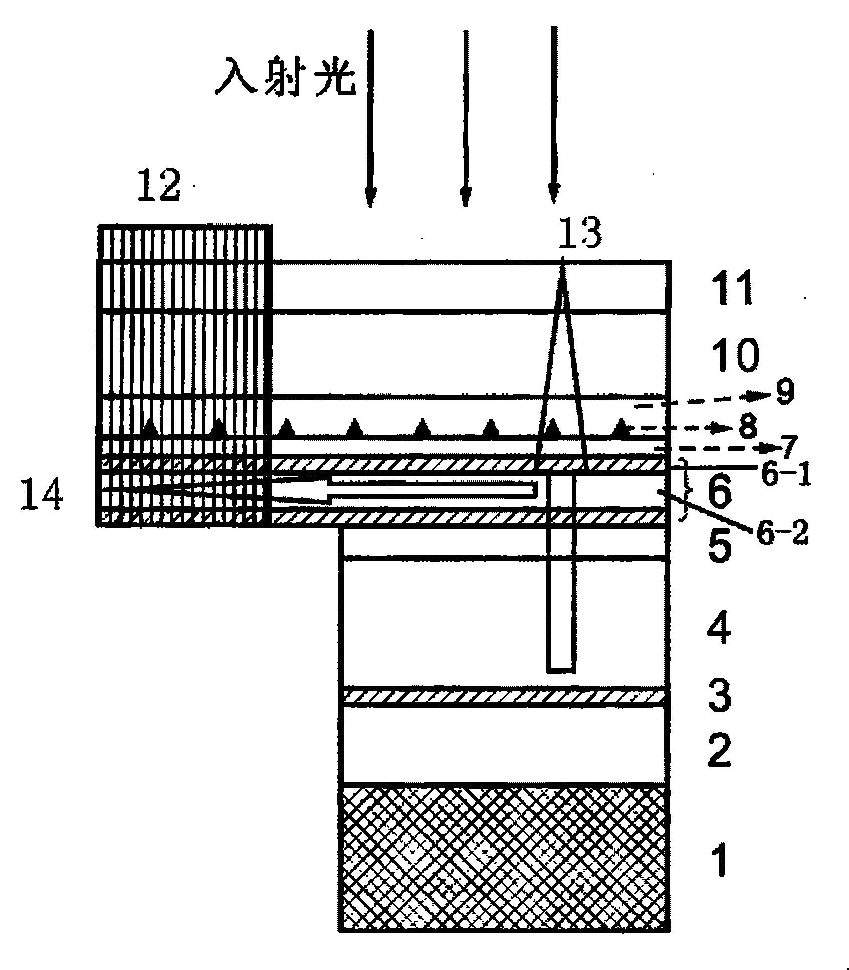
[0029] The structure of the quantum dot resonant tunneling diode with field effect enhancement in this example is shown in Figure 1. The thickness of the GaAs buffer layer 2 is 400nm, the thickness of the AlAs corrosion barrier layer 3 is 15nm, and the n + The GaAs lower electrode layer 4 has a thickness of 430nm and a concentration of 10 18 cm -3 fade to 10 16 cm -3 , the thickness of the first GaAs spacer layer 5 is 20nm, the double barrier structure layer 6 is composed of AlAs potential barrier 6-1 and GaAs potential well 6-2, and the thickness of the AlAs potential barrier layer is 3nm, the thickness of the GaAs potential well is 8nm, the second GaAs spacer layer 7 thickness 2nm, InAs quantum dots 8 density of 1011 cm -2 , intrinsic GaAs quantum dot covering layer 9 thickness 10nm, third GaAs spacer layer 10 thickness 150nm,...
PUM
 Abstract
Description
Claims
Application Information


