Optical scanner for image system

An optical scanning and image technology, applied in parts of TV systems, image communication, color TV parts, etc., can solve problems such as CCDM development obstacles, lower reliability, and large size

Inactive Publication Date: 2009-01-28
E PIN OPTICAL IND
View PDF15 Cites 0 Cited by
  • Summary
  • Abstract
  • Description
  • Claims
  • Application Information

AI Technical Summary

Problems solved by technology

For an A4-sized object to be scanned 10, after the reflected light passes through the reflective lens 12 and the focusing lens 13 to the CCD image sensing component 16, the focal length (Focus Length) is about 1 meter, although the DOF (depth of focus) is relatively large. Can scan a little crumpled paper, but relatively also make CCDM1 bulky; And because the CCD image sensing assembly 16 is smaller than the object 10 to be scanned, it is necessary to focus the relative position of the object 10 to be scanned on the CCD image sensing assembly 16 , which increases the necessity of adjustment in assembly; but the CCD image sensing component 16 can accept low noise ratio S/N, so the colors are richer, as disclosed in JP2006-067504, US2004/263915, etc.
[0004] The CCD image sensing assembly 16 is developed with an array CCD (array CCD) and a linear CCD (linear CCD). The main problem of the optical scanning module CCDM that utilizes the CCD image sensing assembly 16 to form is that the CCD image The sensing component 16 requires additional electronic components to convert the analog signal converted by the CCD image sensing co

Method used


Image

  • Optical scanner for image system
  • Optical scanner for image system
  • Optical scanner for image system

Examples


no. 1 example

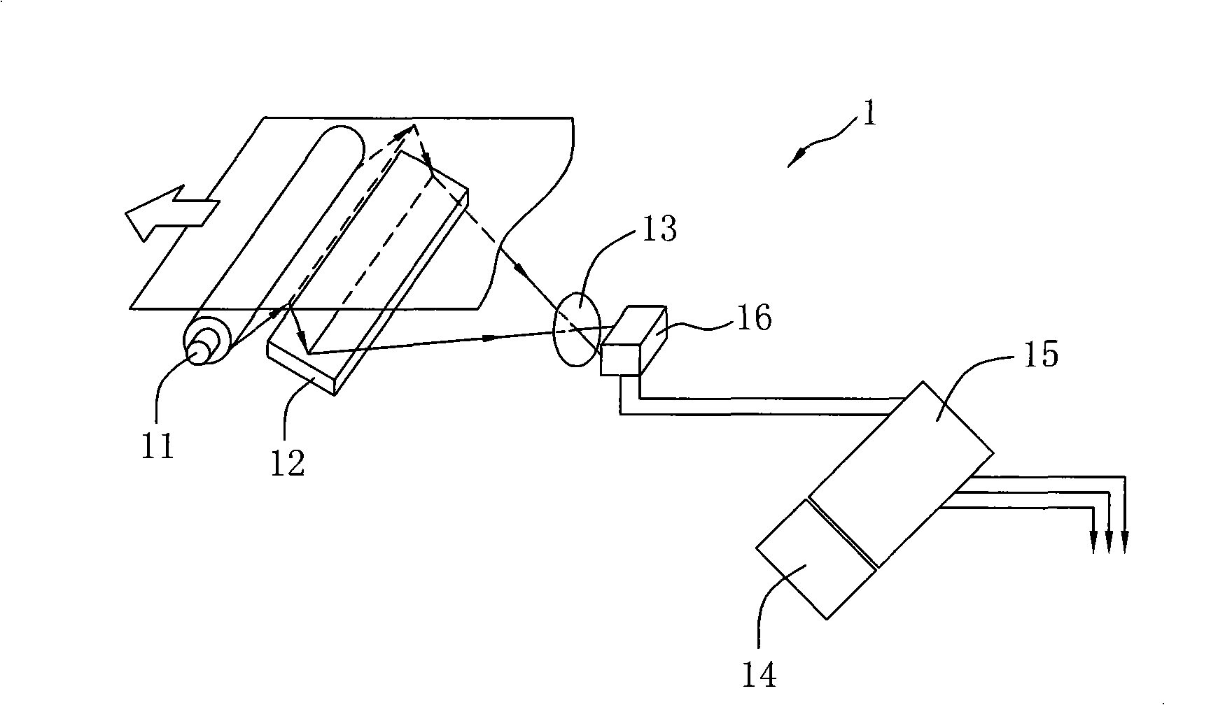
[0028] refer to Figure 5As shown, it is that the optical scanning module (linear CMOSM) 3 of the present invention is applied to a document scanner, and the object 30 to be scanned is a document of A4 size, which is placed on the glass plate of the scanner. The linear CMOSM3 of the invention mainly includes: a CCFL light source 31, which can emit light 311 (light) and irradiate it on the object 30 to be scanned, and be reflected as scanning light 312 (scanning light) by the object 30 to be scanned; Composed of one or several reflective mirrors, the reflective mirror group 32 described in this embodiment is composed of a first reflector 321, a second reflector 322 and a third reflector 323; the scanning light 312 is first irradiated on the first Reflecting mirror 321, the first reflecting mirror 321 refracts the scanning light 312 at the second reflecting mirror 322, and the second reflecting mirror 322 refracts the scanning light 312 at the third reflecting mirror 323, so tha...

no. 2 example

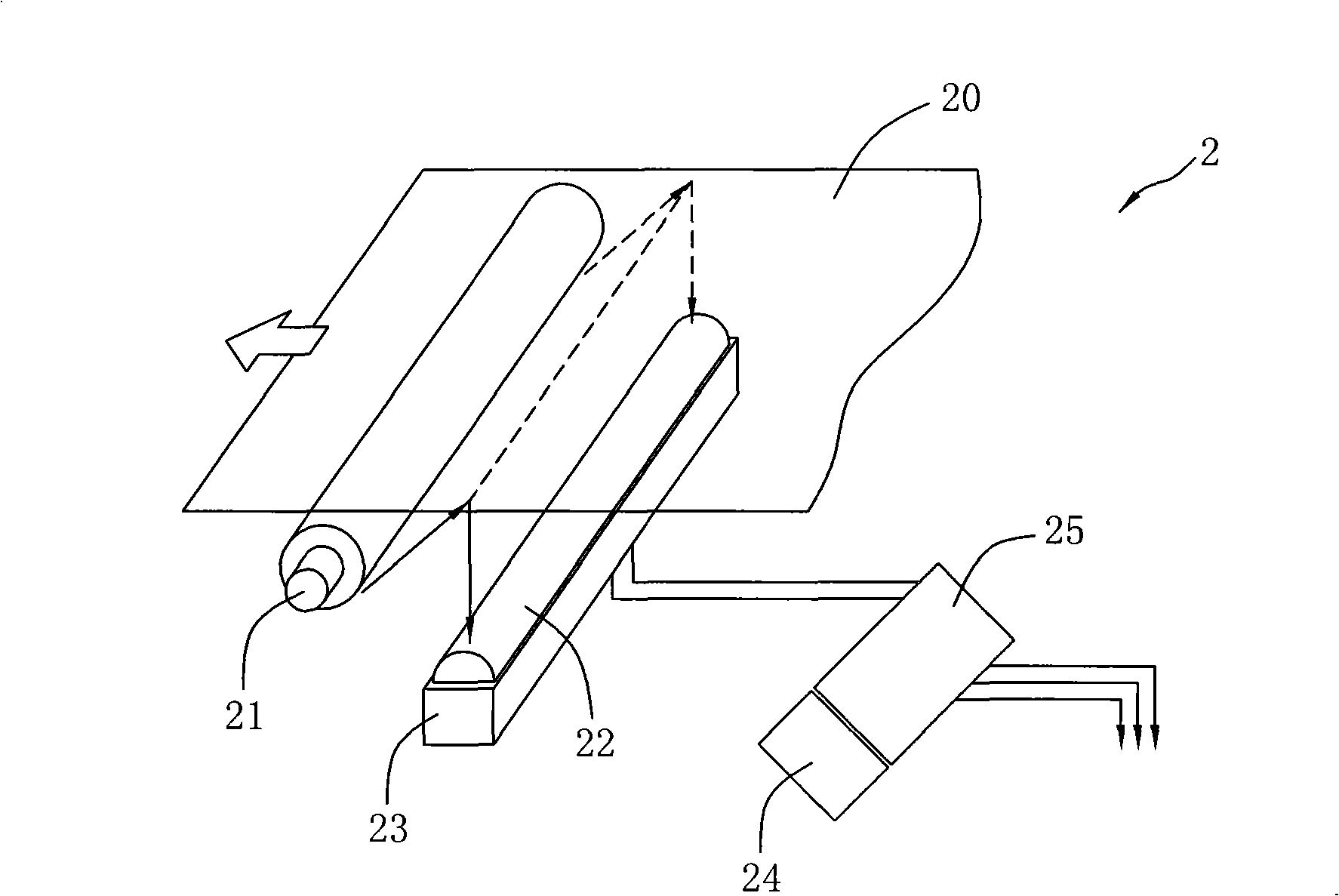
[0037] refer to Figure 10 As shown, the optical scanning module (linear CMOSM) 3 of the present invention can further replace the focusing lens group 33 with an autofocus lens group (AF zooming lens) 35 and an AF control unit 351. Through the The AF control unit 351 can automatically adjust the focusing point of the autofocus lens group (AFzooming lens) 35, so as to improve the convenience of using the linear CMOS M3, and also avoid the unevenness of the surface of the object to be scanned 30 (a three-dimensional object as shown in the figure). Flat and distorted. The auto-focus lens group 35 includes at least two lens groups, at least one of which is movable, and the movement of the lens groups is controlled by the AF control unit 351 (AF Controller), and the distance generated by the relative movement between the lens groups change, so as to automatically focus the scanning light 312 on the focal point and form an image on the linear CMOS image sensing unit 341 . The auto...

no. 3 example

[0040] The light source 31 used by the linear CMOSM3 of the present invention will not be limited as the light source of existing CCDM or CISM, and the light source 31 can be selected to use CCFL, or xenon (Xe) gas lamp or direct-down LED As a light source, this is another effect that the present invention can apply.

[0041] When selecting a cold cathode fluorescent lamp (CCFL) as the light source 31, the light source 31 comprises a CCFL lamp tube and a narrow and long aperture (aperture), and the length of the light source 31 can be set as the scan width of the object to be scanned ( scanning width); the CCFL lamp tube is a mercury discharge lamp tube, when applied to the light source of the present invention, its structure is to coat a fluorescent agent that can emit white light in the lamp tube, and seal a little inert gas and mercury, when the lamp The two ends of the tube are fed with current, and the mercury molecules will generate ultraviolet rays when they are hit by ...


PUM


Abstract

The invention provides an optical scanning module with linear CMOS image sensor, comprising a light source capable of giving out scanning lights, a reflection mirror group, a focus lens group and a linear CMOS image sensor comprising at least one CMOS image sensor unit, and an A/D analog-digital converter, wherein the light source after giving out the light rays is radiated on the object to be scanned, the object to be scanned reflects the light rays which become scanning light rays, and is focalized to the CMOS image sensing unit through the reflection mirror group and the focus lens group as well as is converted into an electronic signal which is converted to the digital signal through the A/D analog-digital converter, a USB signal or an LVDS signal is transmitted to the outside world so as to achieve the high speed scanning and low distortion rate, to have depth of field and to meet the requirement of convenient transportation.

Description

technical field [0001] The present invention relates to an optical scanning device of an image system, especially an optical scanning module (Optical scanning module) composed of a linear complementary metal oxide semiconductor image sensor (linear CMOS image sensor), which can be applied to image Systems such as scanners or MFPs. Background technique [0002] At present, in the imaging system (imaging system), objects are scanned by light and then converted into electronic signals for application, such as scanners, printers, fax machines, or integrated photocopying, scanning, Multi-function printers (MPF, multi-function printers) that integrate printing and faxing are the most common; most of these imaging systems have an optical scanning module (optical scanning module). The above-mentioned light source can emit light onto the picture or text to be scanned or printed, and then receive the reflected light through an image sensor component (image sensor, or image photorecep...

Claims


Application Information

Patent Timeline
IPC IPC(8): H04N5/335H04N5/225
Inventor 徐三伟汪康生林清源
Owner E PIN OPTICAL IND
Why Eureka
Try Eureka