
Aqueous cleaning compositions for semi-conductor copper processing

A cleaning composition, a technology for the composition, applied in the directions of detergent compositions, non-surface-active detergent compositions, semiconductor/solid-state device manufacturing, etc., can solve the problem of copper wire wafer open circuit/short circuit test reliability test deterioration, surface roughness To solve problems such as deterioration of the degree, to achieve the best surface roughness and reduce the number of defects

Active Publication Date: 2009-02-11
EPOCH MATERIAL CO LTD
View PDF12 Cites 0 Cited by
  • Summary
  • Abstract
  • Description
  • Claims
  • Application Information

AI Technical Summary

Problems solved by technology

[0016] With the progress of semiconductor wafer processing, the width of metal wires has been reduced to 32 nanometers, and there are still many problems to be overcome in the new planarization process, such as the surface roughness of the wafer surface with nanometer line width may become worse after processing, and The open / short test (open / short test) and reliability test (reliability test) of the copper wire chip are more prone to deterioration after the line width is reduced

Method used


Image

  • Aqueous cleaning compositions for semi-conductor copper processing

Examples


Embodiment

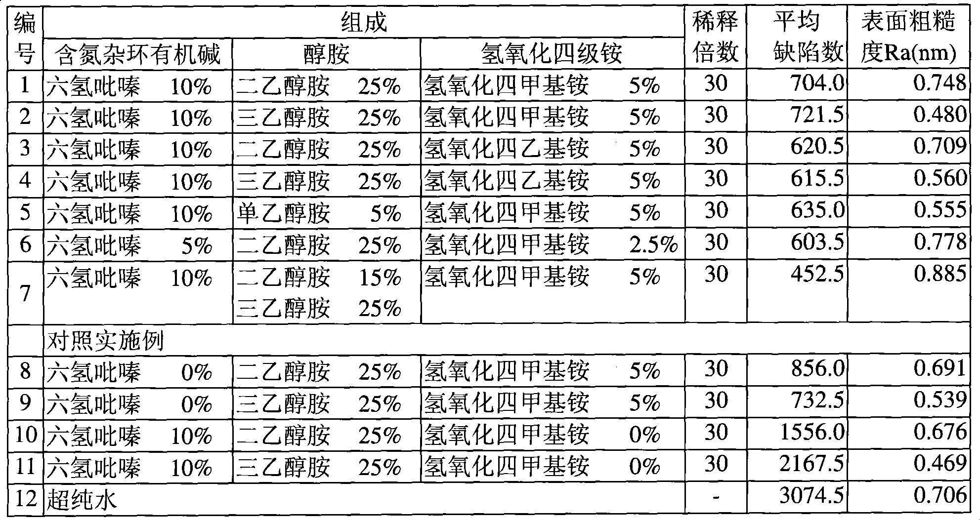
[0030]Cleaning compositions with different compositions were prepared with nitrogen-containing heterocyclic organic bases, alcohol amines, and quaternary ammonium hydroxide. The cleaning compositions were diluted 30 times with ultrapure water on the cleaning machine Ontrak, and the ground copper blank wafers were processed Cleaning, the cleaning time is two minutes, and the cleaning agent flow rate is 600 ml per minute. After cleaning, measure the number of defects on the surface of the copper wafer with a TOPCON WM-1700 wafer particle measuring instrument, and measure the surface roughness (Ra) of the copper wafer with an atomic force microscope (AFM).

[0031] Table 1: Number of surface defects and roughness after cleaning the copper wafer with the cleaning composition

[0032]

[0033] From the results of the above compositions 1 to 11, comparing the cleaning compositions of numbers 1, 8 and 10, and the cleaning compositions of numbers 2, 9 and 11, it can be seen that wh...


PUM


Abstract

The invention relates to a water phase cleaning composition which is used in or after the chemical mechanical planarization during the copper processing of an integrated circuit, and the water phase cleaning composition comprises 0.05 to 20 percent by weight of nitrogen-containing heterocyclic organic base, 0.05 to 50 percent by weight of alkylol amine, 0.01 to 10 percent by weight of quaternary ammonium hydroxide and water. When the water phase cleaning composition is used in or after the planarization process of a semiconductor, the cleaning composition can effectively remove residual pollutants from the surface of a chip and simultaneously give the better surface roughness to the surface of the chip.

Description

technical field [0001] The present invention relates to an aqueous cleaning composition for chemical mechanical planarization (CMP) in integrated circuit copper processing. Background technique [0002] With regard to semiconductor devices, they are currently developing toward smaller line widths and higher product densities. When the minimum line width of an integrated circuit is reduced to below 0.25 microns, the time delay (RC delay) caused by the resistance of the metal wire itself and the parasitic capacitance of the dielectric layer has become the main key affecting the operation speed of the component. Therefore, in order to improve the computing speed of components, the current industry has gradually changed to copper metal wires to replace the traditional aluminum-copper alloy wires for high-end processing below 0.13 microns. [0003] Applying chemical mechanical planarization (CMP) technology to the processing of copper metal wires can not only overcome the proble...

Claims


Application Information

Patent Timeline
IPC IPC(8): C11D7/32H01L21/304
Inventor 陈建清刘文政庄宗宪陈瑞清
Owner EPOCH MATERIAL CO LTD
Learn More