P type silicon carbide device and preparation thereof

A production method and technology of silicon carbide, applied in semiconductor devices, electrical components, circuits, etc., can solve problems such as difficult to determine, difficult to high doping, limited doping concentration, etc., and achieve good ohmic contact performance

Inactive Publication Date: 2009-02-18
NORTH CHINA UNIVERSITY OF TECHNOLOGY
View PDF0 Cites 7 Cited by
  • Summary
  • Abstract
  • Description
  • Claims
  • Application Information

AI Technical Summary

Problems solved by technology

The most commonly used method to obtain a good ohmic contact is heavy doping, which can make the barrier thinner and increase the tunnel current, but for many materials, it is difficult to achieve high doping, and high doping method is used to do The minimum contact resistance obtained is also limited by the doping concentration; in many cases, annealing can form a stable barrier height and low leakage current, which is a better way to form an ohmic contact, but this method is not easy to determine the formed Is the contact an ohmic contact or a Schottky rectifying contact

Method used


Image

  • P type silicon carbide device and preparation thereof
  • P type silicon carbide device and preparation thereof
  • P type silicon carbide device and preparation thereof

Examples


Embodiment Construction

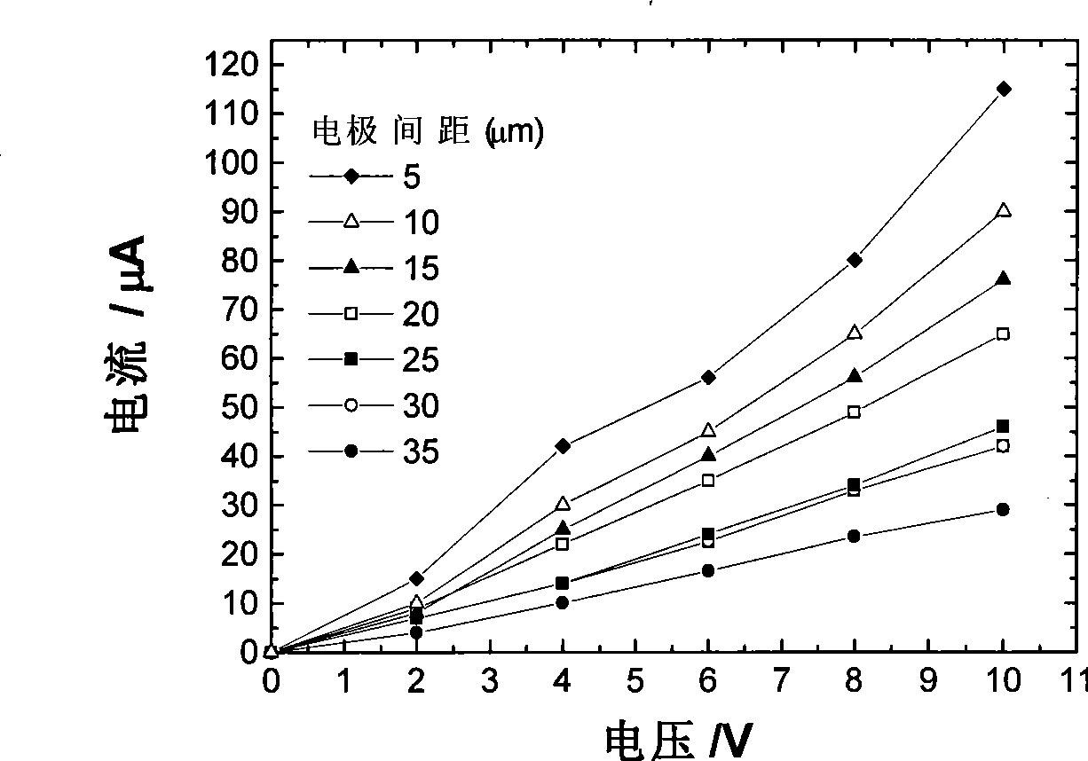
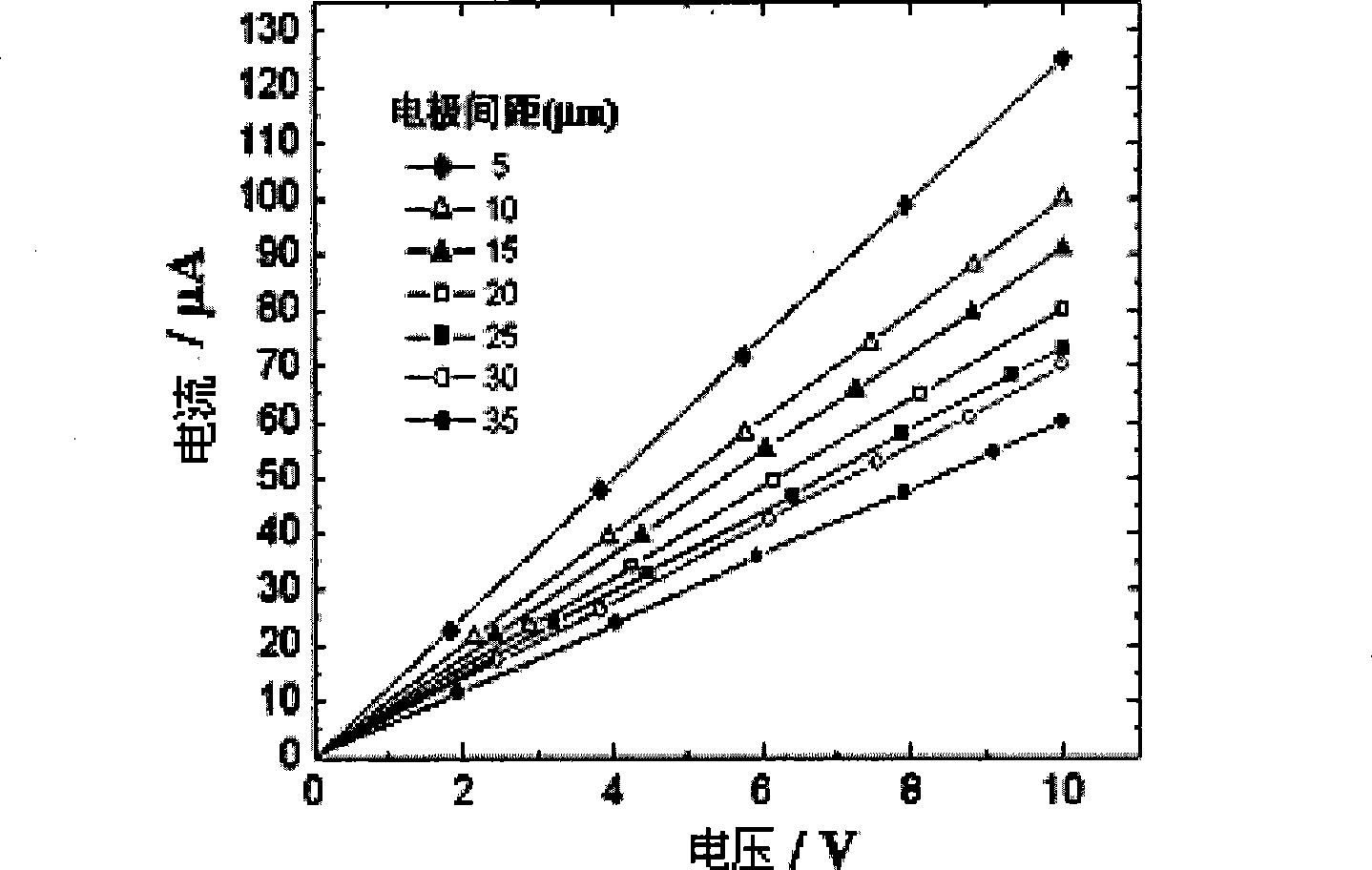
[0014] A preferred embodiment of the P-type silicon carbide device of the present invention includes a silicon carbide layer and an aluminum electrode layer, and a gold nanoparticle layer is arranged between the silicon carbide layer and the aluminum electrode layer. The thickness of the gold nanoparticle layer is 90-110 nanometers, and may be 90, 100, or 110 nanometers. The thickness of the aluminum electrode layer is about 2 microns.

[0015] The manufacturing method of the above-mentioned P-type silicon carbide device of the present invention comprises

[0016] First, a gold nanoparticle layer is deposited on the silicon carbide layer and annealed. The gold nanoparticle layer is deposited on the silicon carbide layer by sputtering. The thickness of the gold nanoparticle layer is estimated to be 100nm. The annealing temperature is 450-710° C., and the annealing time is 8-10 minutes. The protective gas used in the annealing process is nitrogen.

[0017] Three specific embo...


PUM

PropertyMeasurementUnit
thicknessaaaaaaaaaa
thicknessaaaaaaaaaa
thicknessaaaaaaaaaa

Abstract

The invention discloses a P-type silicon carbide apparatus and a manufacturing method thereof. The P-type silicon carbide apparatus comprises a silicon carbide layer and an aluminum electrode layer; a gold nano-particle layer is arranged between the silicon carbide layer and the aluminum electrode layer. The manufacturing method comprises: firstly, depositing the gold nano-particle layer on the silicon carbide layer by using a sputtering method, and carrying out annealing treatment, wherein, the depositing thickness is 100 nanometers, the temperature of the annealing treatment is 450 to 710 DEG C, the annealing time is 8 to 10 minutes, and the protective gas is nitrogen; and then, manufacturing the aluminum electrode layer on the gold nano-particle layer. The manufactured P-type silicon carbide apparatus has better ohmic contact performance.

Description

technical field [0001] The invention relates to a semiconductor technology, in particular to a P-type silicon carbide device and a manufacturing method thereof. Background technique [0002] Due to the wide band gap, high critical electric field strength, large saturated electron velocity and high thermal conductivity of silicon carbide materials, it is suitable for the production of electronic devices such as high temperature, high pressure, high frequency, high power and radiation resistance. ideal material. Ohmic contacts have a linear voltage-current relationship; the resistance is negligible relative to the size of the SiC device. Making a good ohmic contact is one of the important processes for making semiconductor devices, especially for silicon carbide devices that need to be manufactured with high power. How to improve the ohmic contact performance has become the key to restricting the practical use of this kind of device. [0003] A good ohmic contact requires a ...

Claims


Application Information

Patent Timeline
Patent Type & Authority Applications(China)
IPC IPC(8): H01L29/45H01L21/28
Inventor 姜岩峰
Owner NORTH CHINA UNIVERSITY OF TECHNOLOGY
Why Eureka
Try Eureka