Vertical epitaxial structure LED chip and preparation method thereof

A technology of LED chip and epitaxial structure, which is applied to semiconductor devices, electrical components, circuits, etc., can solve the problems of poor substrate peelability, increased production cost, and low peeling yield.

Pending Publication Date: 2022-07-22
JUCAN PHOTOELECTRIC TECH (SUQIAN) CO LTD
View PDF0 Cites 0 Cited by
  • Summary
  • Abstract
  • Description
  • Claims
  • Application Information

AI Technical Summary

Problems solved by technology

[0005] This application provides a vertical epitaxial structure LED chip and its preparation method to solve the problems of poor peeling of the substrate, easy damage to the upper epitaxial structure, resulting in increased leakage rate, poor performance of the LED chip, low peeling yield, and increased production costs.

Method used


Image

  • Vertical epitaxial structure LED chip and preparation method thereof
  • Vertical epitaxial structure LED chip and preparation method thereof
  • Vertical epitaxial structure LED chip and preparation method thereof

Examples


Embodiment Construction

[0059] Embodiments will be described in detail below, examples of which are illustrated in the accompanying drawings. Where the following description refers to the drawings, the same numerals in different drawings refer to the same or similar elements unless otherwise indicated. The implementations described in the following examples are not intended to represent all implementations consistent with this application. are merely exemplary of systems and methods consistent with some aspects of the present application as recited in the claims.

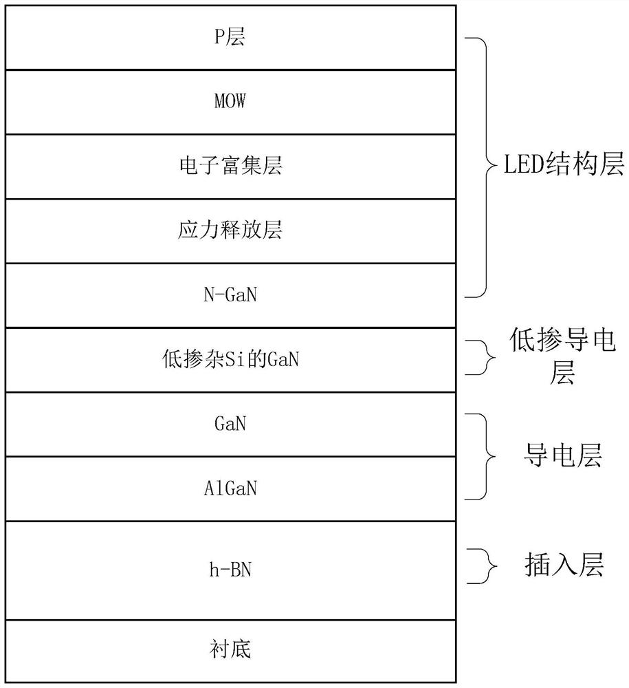
[0060] LED is a light-emitting diode, which is a commonly used light-emitting device. It emits energy through the recombination of electrons and holes. It is widely used in the field of lighting. The core part of the light-emitting diode is a wafer composed of P-type semiconductors and N-type semiconductors, and there is a transition layer between the P-type semiconductors and the N-type semiconductors, which is called a PN junction. Lik...


PUM

PropertyMeasurementUnit
thicknessaaaaaaaaaa
thicknessaaaaaaaaaa

Abstract

The invention provides a vertical epitaxial structure LED chip and a preparation method thereof, the vertical epitaxial structure LED chip comprises a substrate, an insertion layer, a conductive layer, a low-doped conductive layer and an LED structure layer which are sequentially arranged in a laminated manner, and the insertion layer is a hexagonal boron nitride layer; the conductive layer comprises a plurality of gallium nitride aluminum/gallium nitride heterojunction layers. The mutual acting force between the hexagonal boron nitride layered structures is small, and the damage of stripping to the upper epitaxial structure is small. And by utilizing the layered structure characteristic of the hexagonal boron nitride, the laser lift-off technology cannot damage the structure on the hexagonal boron nitride layer, so that the yield of the LED chip is improved. The gallium nitride aluminum/gallium nitride heterojunction structure can play a role similar to a chip DBR (Distributed Bragg Reflector) due to different materials. Moreover, through the design that the silicon-doped concentration of the gallium aluminum nitride/gallium nitride heterojunction layer is gradually reduced, the gallium aluminum nitride/gallium nitride heterojunction layer can be well matched with an electrode, and has good conductive and ohmic contact effects.

Description

technical field [0001] The present application relates to the technical field of LED chips, and in particular, to a vertical epitaxial structure LED chip and a preparation method thereof. Background technique [0002] With the gradual application of LEDs in the field of lighting, the market has higher and higher requirements for the light efficiency of white LEDs (light-emitting diodes); GaN (gallium nitride)-based vertical structure LEDs have single-sided light output, excellent heat dissipation efficiency, and uniform current distribution , improve current congestion, can carry large current injection, make full use of light-emitting layer materials and other advantages. [0003] In the industry, MOCVD (Metal-OrganicChemicalVapourDeposition, metal organic compound chemical vapor deposition) method is mainly used to prepare LED epitaxial wafers, and PSS substrates (Patterned Sapphire Substrate, patterned sapphire substrates) are generally used. A mask for dry etching is gr...

Claims


Application Information

Patent Timeline
Patent Type & Authority Applications(China)
IPC IPC(8): H01L33/12H01L33/10H01L33/14H01L33/06H01L33/32H01L33/36
CPCH01L33/12H01L33/10H01L33/14H01L33/06H01L33/32H01L33/36
Inventor 徐洋洋江汉徐志军黎国昌程虎王文君苑树伟
Owner JUCAN PHOTOELECTRIC TECH (SUQIAN) CO LTD
Why Eureka
Try Eureka