Organic opto-electronic device with protection layer and preparation method thereof

A technology for optoelectronic devices and protective layers, which is applied in the fields of electric solid-state devices, semiconductor/solid-state device manufacturing, photovoltaic power generation, etc., can solve the problems of OLED stability and lifespan, and achieve improved surface properties, improved flatness, and novel structures Effect

Inactive Publication Date: 2009-02-18
UNIV OF ELECTRONIC SCI & TECH OF CHINA
View PDF0 Cites 13 Cited by
  • Summary
  • Abstract
  • Description
  • Claims
  • Application Information

AI Technical Summary

Problems solved by technology

[0003] The difficulties faced in realizing mass production of organic optoelectronic devices including OLEDs mainly include the follo

Method used


Image

  • Organic opto-electronic device with protection layer and preparation method thereof
  • Organic opto-electronic device with protection layer and preparation method thereof
  • Organic opto-electronic device with protection layer and preparation method thereof

Examples


Example Embodiment

[0057] Example 1

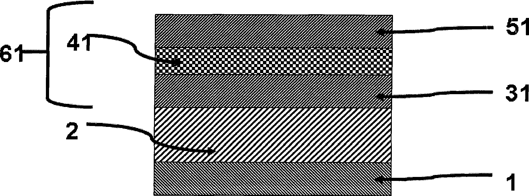
[0058] Such as figure 1 As shown, the substrate 1 and the organic optoelectronic device 2 in the device structure are organic electroluminescence devices, an organic material layer 31, a hydrophilic material layer 41, an organic material layer 51, and a combined layer 61.

[0059] The substrate 1 of the device is PET, the organic optoelectronic device 2 is an organic electroluminescence device, the organic material layer 31 is UV glue, the hydrophilic material layer 41 is calcium oxide, and the organic material layer 51 is UV glue.

[0060] The preparation method is as follows:

[0061] ① Prepare the organic material layer UV glue 300nm on the upper layer of the organic electroluminescent device;

[0062] ②Evaporation or spin-coating a layer of hydrophilic material layer of calcium oxide 500nm on the organic material layer UV glue;

[0063] ③ Deposit a layer of organic material layer UV glue 300nm on the above hydrophilic material layer calcium oxide;

[0064] ...

Example Embodiment

[0065] Example 2

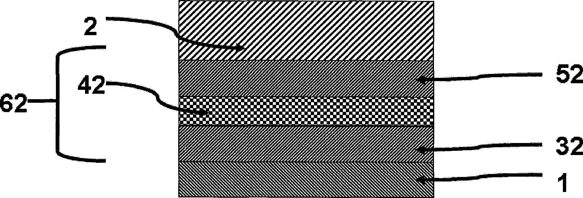
[0066] Such as figure 2 As shown, the substrate 1 and the organic optoelectronic device 2 in the device structure are organic electroluminescent devices, the organic material layer 32, the hydrophilic material layer 42, the organic material layer 52, and the combined layer 62.

[0067] The substrate 1 of the device is PET, the organic optoelectronic device 2 is an organic electroluminescence device, the organic material layer 32 is UV glue, the hydrophilic material layer 42 is calcium oxide, and the organic material layer 52 is UV glue.

[0068] The preparation process of the device is as follows:

[0069] ① Prepare the organic material layer UV glue 300nm on the upper layer of the substrate;

[0070] ②Prepare a layer of hydrophilic material layer of calcium oxide 500nm on the above-mentioned organic material layer UV glue;

[0071] ③ Deposit a layer of organic material layer UV glue 300nm on the above hydrophilic material layer calcium oxide;

[0072] ④Repeat ...

Example Embodiment

[0074] Example 3

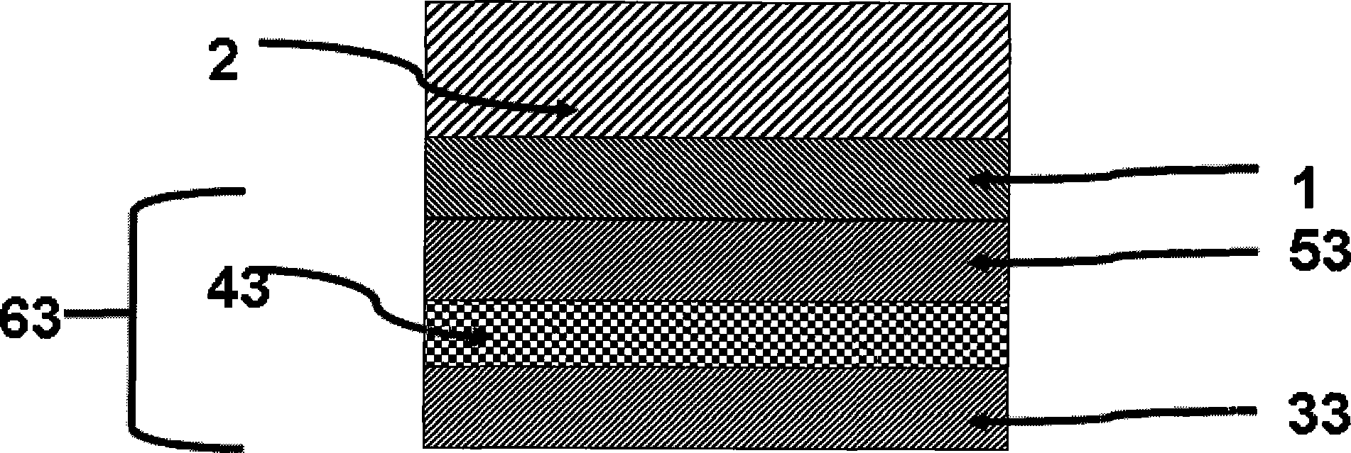
[0075] Such as image 3 As shown, the substrate 1 and the organic optoelectronic device 2 in the device structure are organic thin film transistors, an organic material layer 33, a hydrophilic material layer 43, an organic material layer 53, and a combined layer 63.

[0076] The substrate 1 of the device is PET, the organic optoelectronic device 2 is an organic thin film transistor, the organic material layer 33 is UV glue, the hydrophilic material layer 43 is calcium oxide, and the organic material layer 53 is UV glue.

[0077] The preparation process of the device is similar to that of Example 2.


PUM


Abstract

This invention discloses an organic photoelectron component with protective layer, including a substrate and an organic photoelectron component, further including a protective layer consisting of n combined layers, wherein n is the integer and is not smaller than 1 and not greater than 100. The combined layer is composed of three modes: an organic material layer/hydrophilic material layer/organic material layer or an organic material layer/hydrophilic material layer or hydrophilic material layer/ organic material layer. The position relationship of the combined layers in the protective layer includes: setting at one position or multiple positions of the upper layer, the lower layer, the periphery of the organic photoelectron component; setting between the substrate and the organic photoelectron component or at one side of the substrate. The component is capable of conquering the shortness existed in the current technology and has novel structure; the flatness of the substrate surface is improved. The bonding property of the protective layer solves the problem of connection degree between components and effectively prevents the water and oxygen entering into the inner part of the component.

Description

technical field [0001] The invention relates to the technical field of organic optoelectronic devices, in particular to an organic optoelectronic device with a protective layer. Background technique [0002] Today, with the development of multimedia technology and the advent of the information society, the requirements for the performance of flat panel displays are getting higher and higher. Recently, three new display technologies have emerged: plasma display, field emission display and organic electroluminescent display (OLED), all of which have made up for the shortcomings of cathode ray tubes and liquid crystal displays to a certain extent. Among them, organic electroluminescent displays have a series of advantages such as active light emission, low-voltage DC drive, full curing, wide viewing angle and rich colors. Compared with liquid crystal display devices, organic electroluminescent devices have broad application prospects and are viewed as One of the most competiti...

Claims


Application Information

Patent Timeline
IPC IPC(8): H01L51/00H01L51/50H01L51/52H01L51/56H01L51/05H01L51/10H01L51/40H01L51/42H01L51/44H01L51/48
CPCY02E10/549
Inventor 蒋亚东于军胜李璐张磊
Owner UNIV OF ELECTRONIC SCI & TECH OF CHINA
Why Eureka
Try Eureka