Methods and apparatuses for manufacturing geometric multicrystalline cast silicon and geometric multicrystalline cast silicon bodies for photovoltaics
A manufacturing method, polysilicon technology, applied in new forms of cast silicon, manufacturing cast silicon for optoelectronic applications, can solve the problems of reduced cell efficiency and low efficiency of photovoltaic cells, etc.
- Summary
- Abstract
- Description
- Claims
- Application Information
AI Technical Summary
Problems solved by technology
Method used
Image
Examples
Embodiment approach
[0077] Therefore, the orientation of the seed crystals used to form the silicon in the crucible can be selected so that a specific grain boundary is formed in the cast geometric polysilicon, and this grain boundary surrounds the geometric shape. In contrast to the embodiments of the present invention, known casting methods involve the casting of polycrystalline grains in an uncontrolled manner by the directional solidification of a completely molten silicon substance. The resulting crystal grains have a substantially random orientation and size distribution. The random grain orientation makes it difficult to texture the silicon surface effectively. In addition, it has been shown that, as a natural product of general growth techniques, kinks in the grain boundaries often form the nuclei of structural defects, which involve clusters or lines of dislocations. These dislocations and the impurities often attracted by them cause rapid recombination of the electrical carrier and deterior...
Embodiment 1
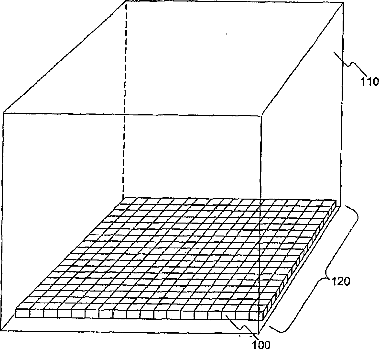
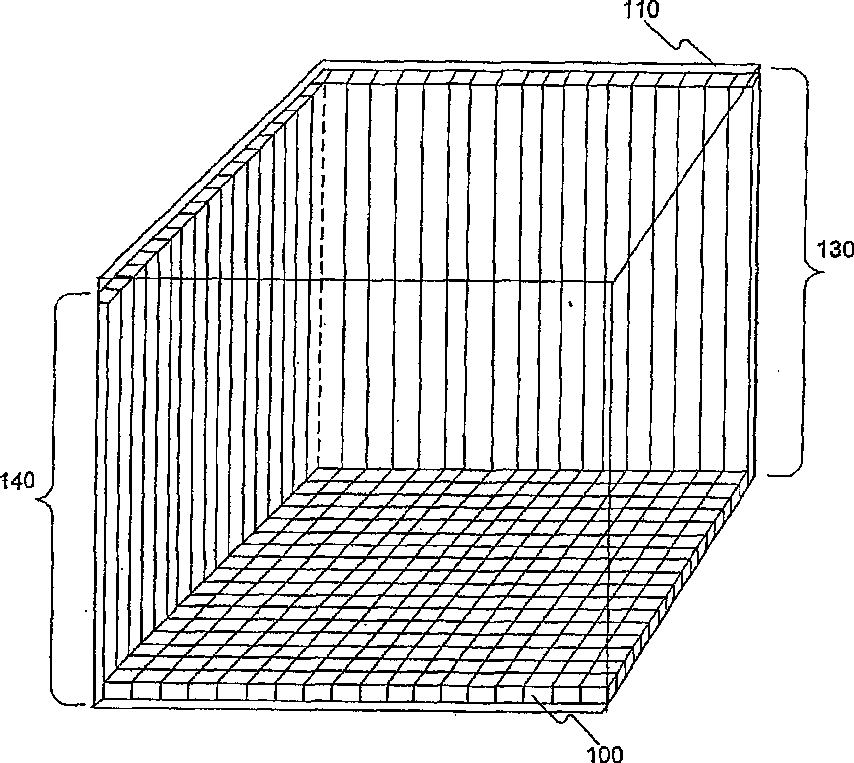
[0096] Seed crystal preparation: Use a diamond-coated band saw to cut out pure Czochralski (CZ) silicon (single crystal) ingots along the length. The pure Czochralski silicon is purchased from MEMC, Inc. and has 0.3ppma of boron to make the crystal The rod has a square cross-section measuring 14 cm on each side. Use the same saw to cut the obtained single crystal silicon block from the cross section into a flat plate with a thickness of about 2 cm to about 3 cm. These plates are used as single crystal silicon seeds or "seeds". Maintain the polar orientation of the (100) crystal of the silicon ingot. Then, the obtained single crystalline silicon plate is arranged on the bottom of the quartz crucible, so that the (100) direction of the plate faces upward, and the (110) direction is kept parallel to one side of the crucible. The quartz crucible has a square cross-section, 68 cm on the side, about 40 cm in depth, and about 1.8 cm in wall thickness. The plates are arranged at the botto...
Embodiment 2
[0100] Seed crystal preparation: seeding was performed as in Example 1, except that the single crystal silicon seed crystal was cut so that half of the seed crystal had a (110) direction at 45 degrees to the side surface of the square seed crystal, and the other half At an angle of about 20 degrees. At the bottom of the crucible, the square slices are layered in a grid pattern, and two different seed crystal orientations are alternated, that is, the (110) direction and the crucible sidewall orientation form an angle of 45 degrees and 20 degrees. Relative to each other, the seed crystals have an orientation difference of 25 degrees or 155 degrees. However, due to the size mismatch of the square-shaped seeds, some voids in the seed layer are not covered. The crucible measures approximately 33 cm on each square side and is approximately 22 cm high.
[0101] Casting: A crucible containing seed crystals and a separate crucible containing a total of 56 kg of raw silicon blocks are loade...
PUM
| Property | Measurement | Unit |
|---|---|---|
| Width | aaaaa | aaaaa |
| Size | aaaaa | aaaaa |
| Surface area | aaaaa | aaaaa |
Abstract
Description
Claims
Application Information


