Anisotropic etching method

An anisotropic, etching gas technology, used in the manufacture of discharge tubes, electrical components, semiconductor/solid-state devices, etc., can solve problems such as unexpected mechanical design, incomplete anisotropic contour, influence, etc., to increase practical performance, widening the surface temperature range, and simplifying the process parameters

Inactive Publication Date: 2009-03-04
ALCATEL LUCENT SAS
View PDF3 Cites 6 Cited by
  • Summary
  • Abstract
  • Description
  • Claims
  • Application Information

AI Technical Summary

Problems solved by technology

[0014] Finally, the slightest difference in substrate temperature regulation can lead to one or other of the above-mentioned conditions, the effect of which will produce an incompletely anisotropic profile
The temperature of the substrate holder is uniform to better than ±1°C, and no further mechanical design improvements are currently expected to further improve this uniformity

Method used


Image

  • Anisotropic etching method
  • Anisotropic etching method

Examples


Embodiment Construction

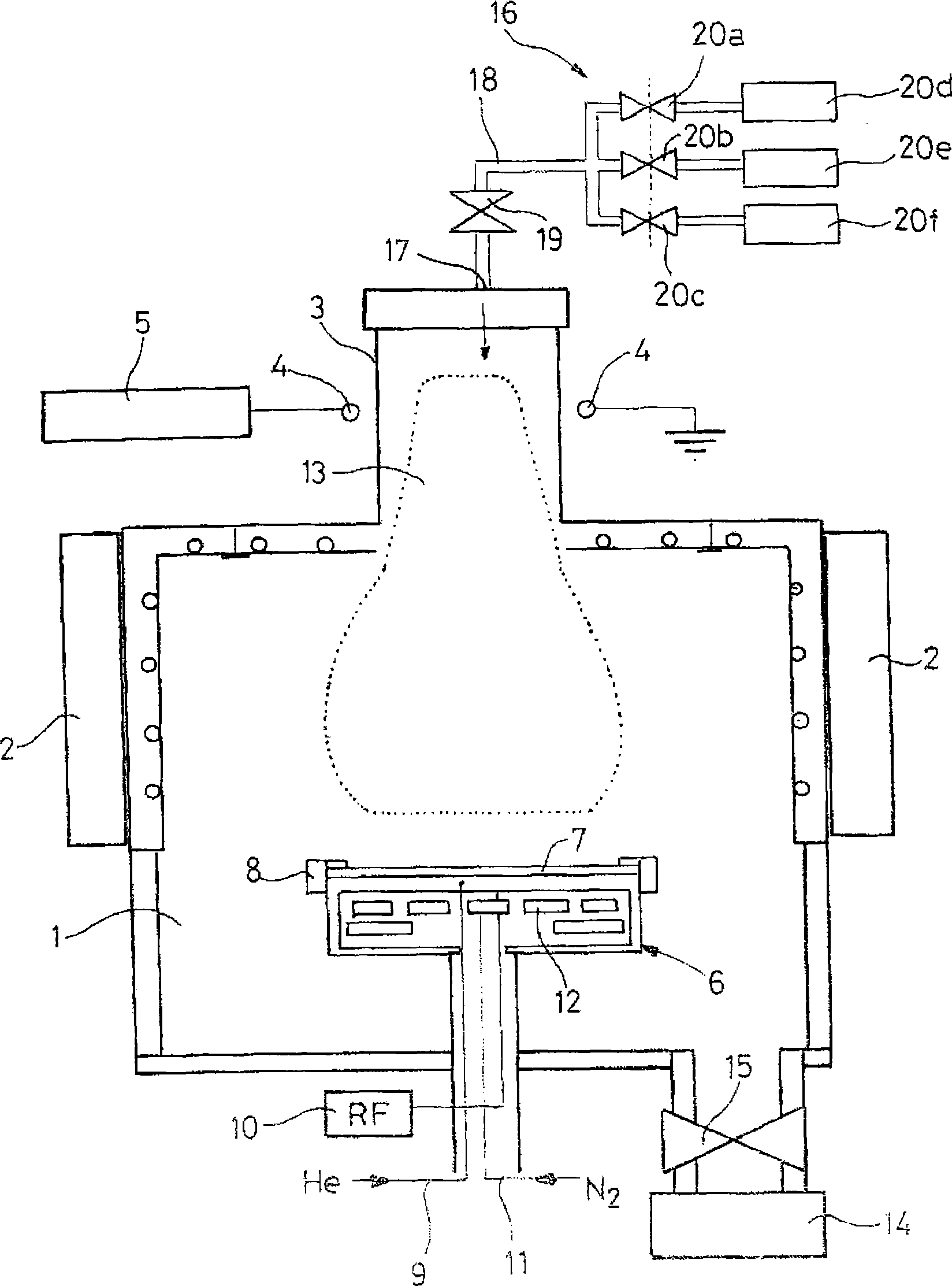
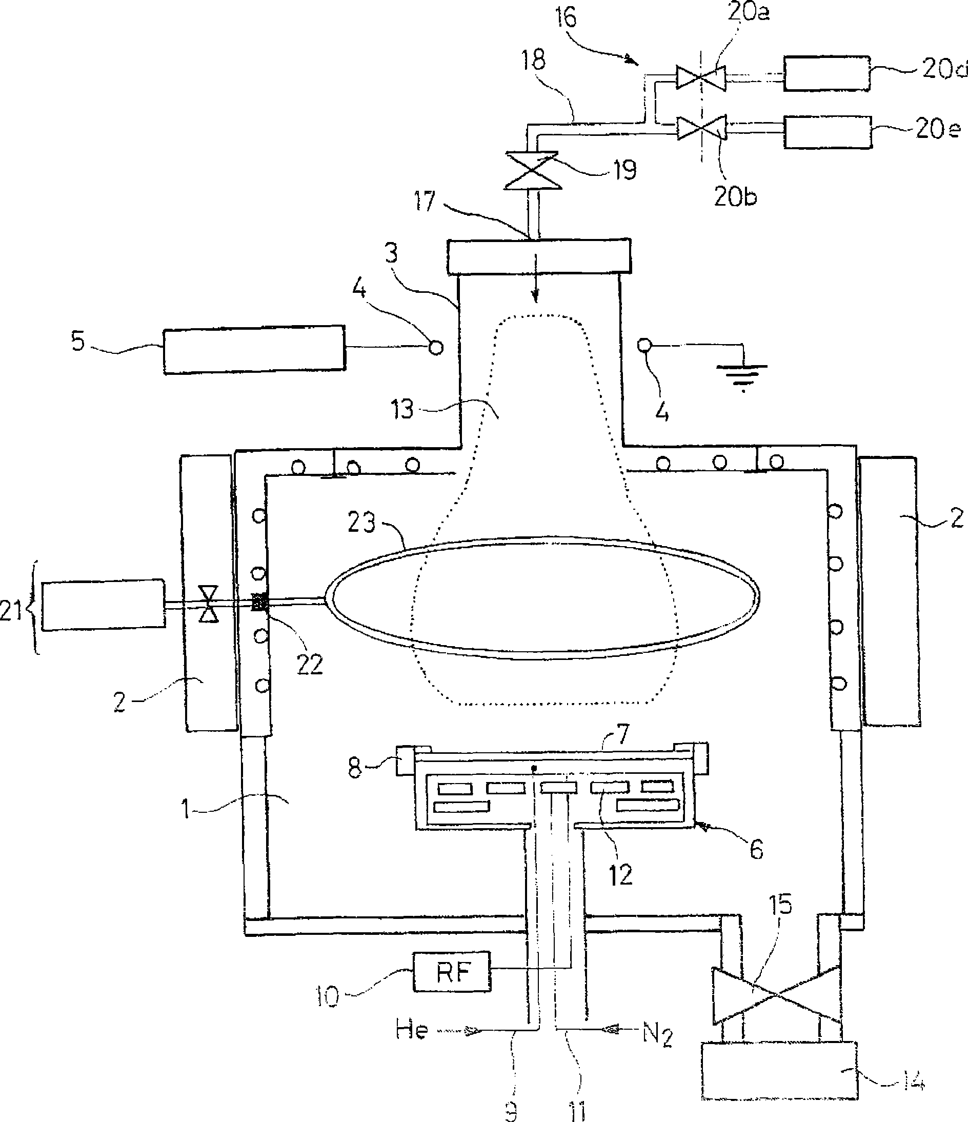
[0043] figure 1 The apparatus shown in is a plasma etcher comprising a processing chamber 1 surrounded by permanent magnets 2 arranged in multipoles to reduce electron losses at the chamber walls. The chamber 1 is in communication with a plasma source whose conduit 3 of dielectric material in which the plasma is formed is surrounded by a coupling electrode 4 to which is supplied a radio frequency (RF) alternating current generated by an RF generator 5, RF The generator 5 provides RF (13.56 MHz) power P of 500W to 2000W.

[0044] Chamber 1 houses a substrate holder 6 . The approximately 100 mm thick substrate 7 to be etched is fixed to the substrate holder 6 by mechanical or electrostatic means, here mechanically for example with a ring 8 . The substrate 7 is separated from the substrate holder 6 by a helium membrane 9 . A bias voltage U of 20V to 60V, preferably 50V is applied to the substrate 7 by means of an RF (13.56MHz) or low frequency (50-500Hz) generator 10 . By cir...


PUM


Abstract

The subject of the present invention is a process for the anisotropic etching of a silcon substrate at very low temperature by a high-density fluorinated gas plasma, characterized in that the plasma is formed from a gas mixture comprising a fluorine-containing etching gas, an oxygen-containing passivation gas and a chlorine-containing reaction gas, in which process the respective ratios of the flow rate of the passivation gas and the flow rate of the reaction gas to the flow rate of the etching gas are less than 0.15 by volume. Preferably, the fluorine-containing etching gas is sulphur hexafluoride SF6, the oxygen-containing passivation gas is chosen from oxygen O2, ozone O3 and sulphur dioxide SO2, and the chlorine-containing reaction gas is silicon tetrachloride SiCl4.

Description

technical field [0001] The present invention relates to an anisotropic etching method for producing tiny reliefs on the surface of a semiconductor substrate, especially a silicon substrate, using a high-density fluorinated gas plasma at a very low temperature, for the manufacture of semiconductor components and Microsystems for microelectromechanical systems (MEMS) and micro-optoelectromechanical systems (MOEMS). Background technique [0002] These microsystems require deep and highly anisotropic etching with high selectivity and high etch rates. Technologies based on non-toxic, non-corrosive and simple chemistry are preferred. [0003] Fluorine-based etching gas plasmas are typically used to generate maximum fluorine ions and atoms, enabling high etch rates for silicon. Fluoride ions and atoms are known to react with silicon spontaneously and exothermically to corrode isotropically. However, to be more precise, the goal is to obtain a figure whose walls are as vertical a...

Claims


Application Information

Patent Timeline
Patent Type & Authority Applications(China)
IPC IPC(8): H01L21/306
CPCH01L21/3065H01J2237/2001H01J37/321
Inventor M·皮埃什
Owner ALCATEL LUCENT SAS
Why Eureka
Try Eureka