Organic light emitting device using high conductive hole transport material as hole transport layer

A technology of hole transport materials and electroluminescent devices, which is applied in the direction of electric solid devices, semiconductor devices, semiconductor/solid device manufacturing, etc., can solve the problems of hindering hole injection, expensive, complicated preparation process, etc., and achieve brightening The effect of low voltage and high efficiency

Inactive Publication Date: 2009-03-11
CHANGCHUN INST OF APPLIED CHEMISTRY - CHINESE ACAD OF SCI
View PDF3 Cites 31 Cited by
  • Summary
  • Abstract
  • Description
  • Claims
  • Application Information

AI Technical Summary

Problems solved by technology

Fluorinated tetracyanoquinodimethane (referred to as F 4 -TCNQ) is a kind of hole-type dopant commonly used at present, however, F 4 - TCNQ is very expensive, and the doping concentration needs to be precisely controlled, usually less than 4%. At high doping concentration, F 4 -TCNQ hinders hole injection, so that the device efficiency cannot be improved
Obviously, strictly controlling the doping concentration complicates the fabrication process of the device

Method used


Image

  • Organic light emitting device using high conductive hole transport material as hole transport layer
  • Organic light emitting device using high conductive hole transport material as hole transport layer
  • Organic light emitting device using high conductive hole transport material as hole transport layer

Examples


Embodiment 1

[0028] The 2-TNATA, TCTA, TDAPB, TDATA, NPD, TPD, s-TAD, m-MTDATA used are commercial products. The conductive film indium tin oxide ITO is used as the electrode 2 to cover the glass substrate 1, and the glass substrate containing ITO is also a commercial product.

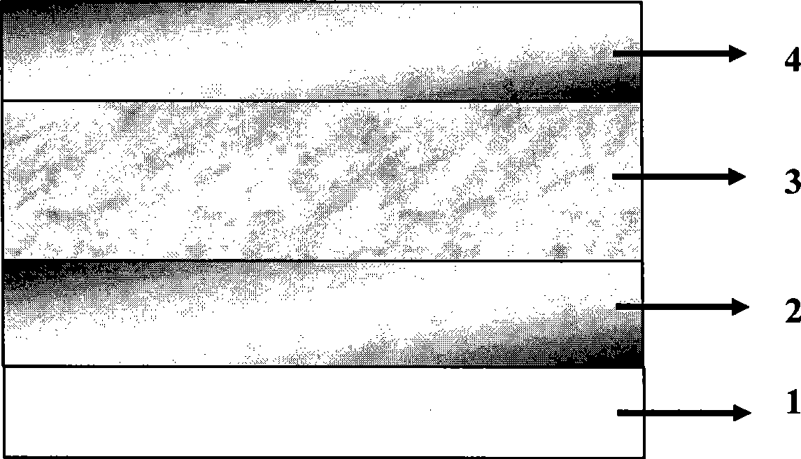
[0029] Diode structure composed of metal oxide doped hole transport material see figure 2 . Clean the ITO on the ITO glass first, dry it with nitrogen gas, and then treat it with oxygen plasma for 2 minutes. Then, in a vacuum of 1-5 x 10 -4 In Pa's coating system, a 100nm-thick metal oxide-doped hole transport material is evaporated on the processed ITO electrode as the active layer 3 . The organic host material in the metal oxide doped hole transport material is any one of 2-TNATA, TCTA, TDAPB, TDATA, NPD, TPD, s-TAD, m-MTDATA, and the metal oxide is pentoxide Vanadium (V 2 o 5 ), molybdenum trioxide (MoO 3 ), tungsten trioxide (WO 3 ), and finally deposit metal aluminum (Al) on the organic semiconductor ...

Embodiment 2

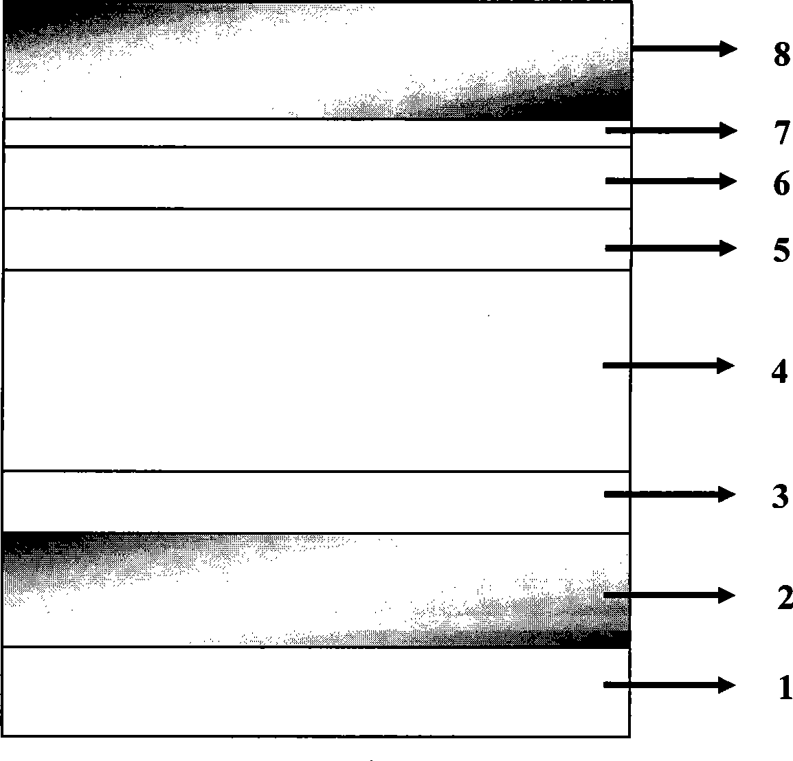
[0035] Structure of organic electroluminescent devices with high conductivity metal oxide doped organic hosts as hole injection transport layer see figure 1 . Clean the ITO on the ITO glass first, dry it with nitrogen gas, and then treat it with oxygen plasma for 2 minutes. After that, in a vacuum of 1-5×10 -4 In Pascal's coating system, 30 nanometers thick MoO is sequentially evaporated on the processed ITO electrode 2 3 Doped NPB hole injection layer 3, 100nm thick NPB hole transport layer 4, 30nm thick C545T doped Alq 3 The light-emitting layer of 5, 30nm thick Alq 3 Electron transport layer 6, 1nm thick lithium fluoride buffer layer 7 and 200nm thick A1 electrode 8, prepared as ITO / MoO 3 :NPB / NPB / C545TAlq 3 / Alq 3 / LiF / Al organic electroluminescent devices. Organic electroluminescent devices with an active area of ​​25 mm2, MoO 3 The doping concentration in NPB was 10% by weight. attached image 3 b shows the current density-brightness-voltage characteristic curv...

Embodiment 3

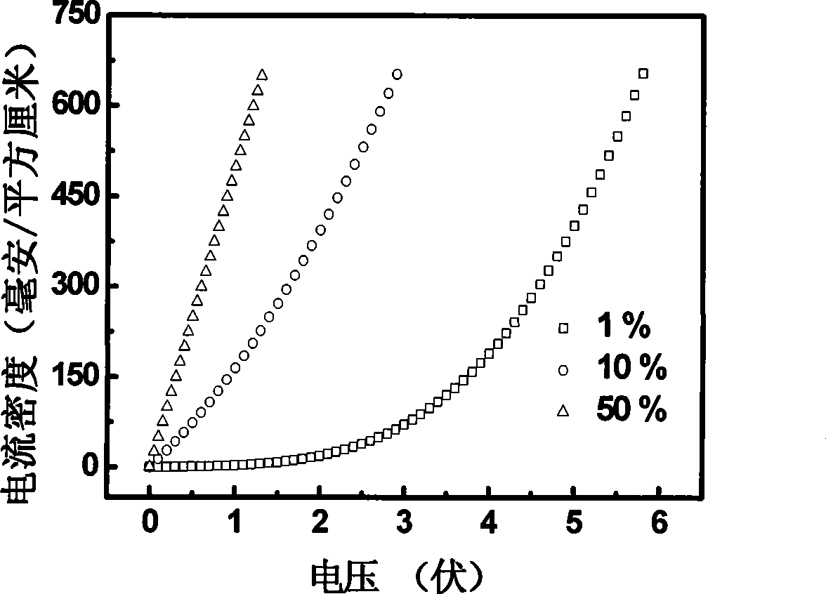
[0037] Structure of organic electroluminescent devices with high conductivity metal oxide doped organic hosts as hole injection transport layer see figure 1 . Clean the ITO on the ITO glass first, dry it with nitrogen gas, and then treat it with oxygen plasma for 2 minutes. After that, in a vacuum of 1-5×10 -4 In Pascal's coating system, 30 nanometers thick MoO is sequentially evaporated on the processed ITO electrode 2 3 Doped NPB hole injection layer 3, 60nm thick NPB hole transport layer 4, 30nm thick C545T doped Alq 3 The light-emitting layer of 5, 30nm thick Alq 3 The electron transport layer 6, the lithium fluoride buffer layer 7 with a thickness of 1nm and the Al electrode 8 with a thickness of 200nm are prepared into a structure of ITO / MoO 3 :NPB / NPB / C545TAlq 3 / Alq 3 / LiF / Al organic electroluminescent devices. Organic electroluminescent devices with an active area of ​​25 mm2, MoO 3 The doping concentration in NPB was 1% by weight. The turn-on voltage of the ...


PUM

PropertyMeasurementUnit
thicknessaaaaaaaaaa
current efficiencyaaaaaaaaaa
energy conversion efficiencyaaaaaaaaaa

Abstract

The invention relates to an organic electroluminescent device which utilizes a high-conductivity hole-transporting material as the hole-transporting layer. The hole-transporting layer of the high-conductivity hole-transporting material is formed by doping an organic main body material and high-conductivity metal oxide. The metal oxide doped with a hole-filling transporting layer of the organic main body has very high conductivity, and the conductivity is between 10<-10> to 10<-6>s/cm; the electroluminescent device has the advantages of low turn-on voltage and high efficiency, the turn-on voltage is between 2.5-2.8 volts, the maximum current efficiency is 15.4-18.5 candelas/ampere (cd/A), and the maximum power efficiency is between 14.1-21.4 lumens/watt (lm/W).

Description

technical field [0001] The invention relates to an organic electroluminescent device using a high-conductivity hole-transporting material as a hole-transporting layer and a preparation method thereof. Background technique [0002] Organic electroluminescent display is regarded as the most popular emerging display technology in the flat panel display industry, and has been extensively researched. Compared with inorganic electroluminescent devices, organic electroluminescent devices have a wide range of material selection, can realize full-color display from blue light region to red light region, low driving voltage, high luminous brightness and luminous efficiency, wide viewing angle, and fast response speed. Fast, simple manufacturing process, low cost, and easy to realize large-area and flexible display, etc., so it has developed rapidly in the past 20 years. At present, the research in the field of organic electroluminescent display devices is no longer limited to academi...

Claims


Application Information

Patent Timeline
Patent Type & Authority Applications(China)
IPC IPC(8): H01L51/50H01L51/54C09K11/06
Inventor 马东阁乔现锋王凤霞熊涛
Owner CHANGCHUN INST OF APPLIED CHEMISTRY - CHINESE ACAD OF SCI
Why Eureka
Try Eureka