Process for growing high-quality monocrystal indium nitride thin-film having double buffering layers

An indium nitride film, double buffer layer technology, applied in electrical components, semiconductor/solid-state device manufacturing, circuits, etc., can solve the problems of low ammonia cracking efficiency and insufficient source of five groups

Inactive Publication Date: 2009-03-18
XIAMEN CHANGELIGHT CO LTD
View PDF0 Cites 12 Cited by
  • Summary
  • Abstract
  • Description
  • Claims
  • Application Information

AI Technical Summary

Problems solved by technology

Because the growth temperature of InN is relatively low (the reason is that the saturated vapor pressure of InN is relatively high), and in the lower temperature range, the cracking efficiency of ammonia gas is very low, resulting in insufficient V group sources for the synthesis of InN, and part of In is formed. Metallic In appears on the sample surface

Method used


Image

  • Process for growing high-quality monocrystal indium nitride thin-film having double buffering layers
  • Process for growing high-quality monocrystal indium nitride thin-film having double buffering layers
  • Process for growing high-quality monocrystal indium nitride thin-film having double buffering layers

Examples


Embodiment Construction

[0025] specific implementation plan

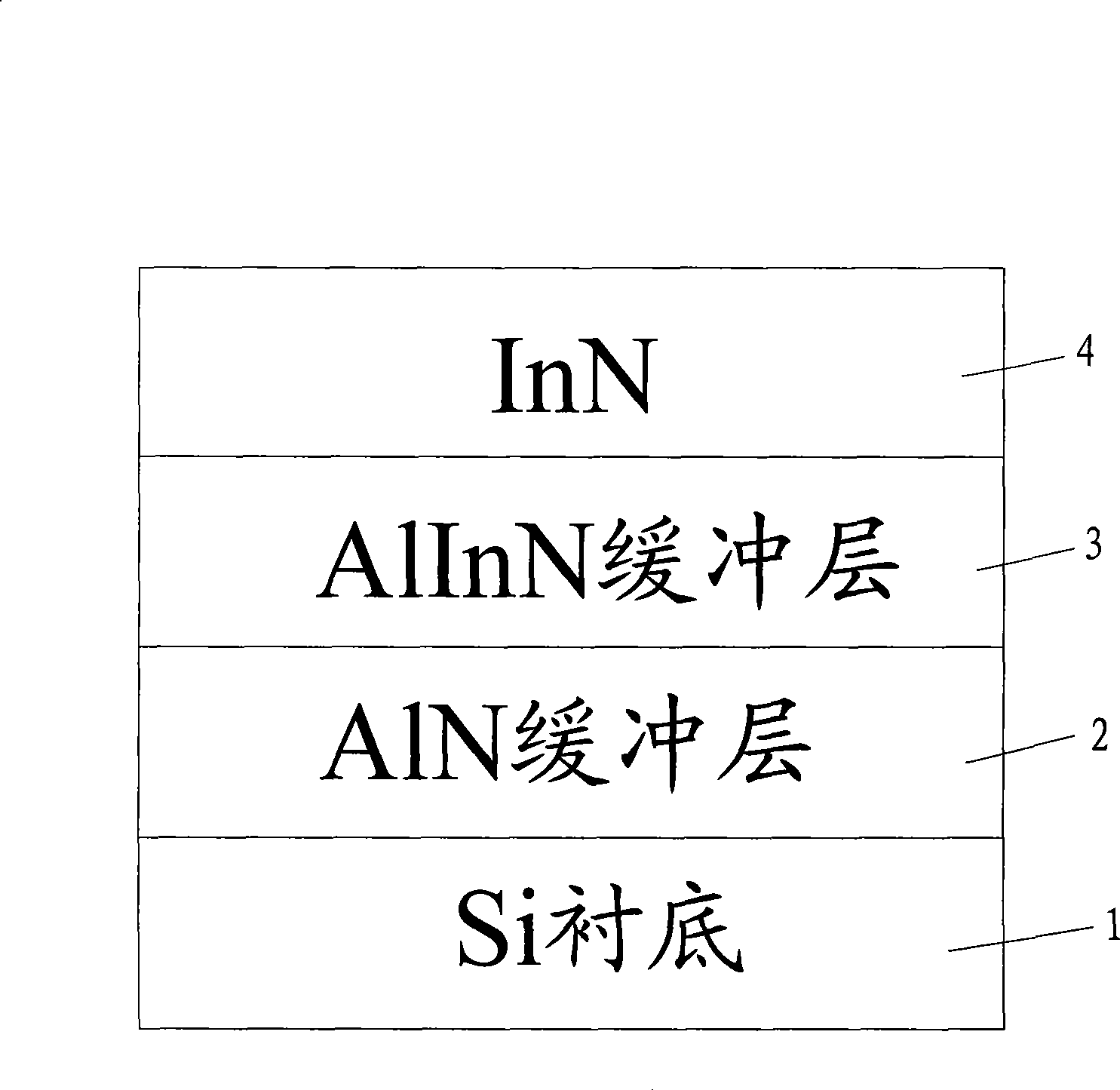
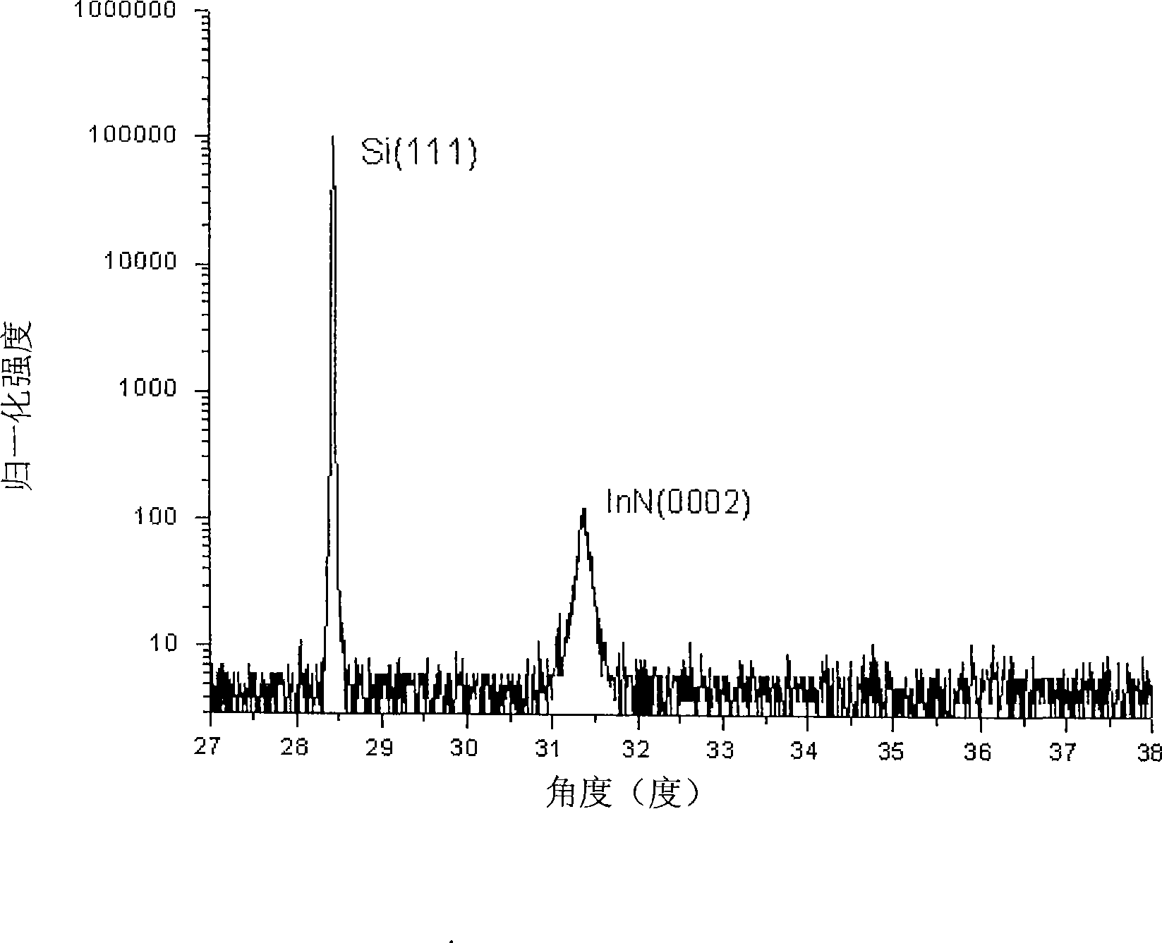
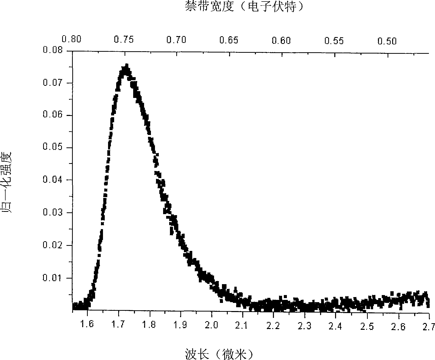
[0026] Such as figure 1 As shown, a method for growing high-quality single-crystal InN films with double buffer layers in the present invention is to utilize MOCVD (metal organic chemical vapor deposition) technology to grow AlN buffer layers 2 on silicon (Si) substrate 1. It is one of the keys of the present invention, continue to grow AlInN buffer layer 3 on AlN buffer layer 2, AlInN buffer layer 3 can be a layer of AlInN buffer layer of single composition, or a layer of AlInN buffer layer of graded composition, or different The multi-layer AlInN buffer layer of the composition, which is the second key of the present invention, finally grows the InN single crystal epitaxy 4 .

[0027] Concrete growth of the present invention comprises the following steps:

[0028] 1. In the MOCVD system, dehydrate the Si substrate 1 at a temperature of 300°C-1000°C, the carrier gas is hydrogen, the treatment time is 10 minutes-15 minutes, and the pr...


PUM


Abstract

The invention discloses a process for growing single-crystal nitriding indium films with high quality and double buffer layers, which comprises growing an AlN buffer layer on a silicon substrate through utilizing the MOCVD technology, continuously growing an AlInN buffer layer on the AlN buffer layer, finally growing InN single-crystal epitaxy, wherein the AlInN buffer layer can be an AlInN buffer layer with single component or an AlInN buffer layer with gradually varied components, wherein In component is gradually increased in a linear change, or be a multi-layer AlInN buffer layer with different components, wherein In component in each layer is gradually increased in a linear change. The process can increase the crystal quality of the InN single-crystal exiptaxy.

Description

[0001] technical background [0002] The invention relates to a method for growing indium nitride InN by MOCVD (metal organic chemical vapor deposition) technology, in particular to a method for growing a high-quality single-crystal InN thin film with double buffer layers. Background technique [0003] Group III-V nitrides as third-generation semiconductor materials: gallium nitride GaN, indium nitride InN, aluminum nitride AlN and their alloy materials are all direct bandgap semiconductor materials with a large forbidden band distribution range, covering from The band from red light to ultraviolet can be used to make light-emitting diodes, lasers, detectors and solar cells, etc., and has a wide range of applications in full-color display white light lighting, high-density storage, and ultraviolet detection. On the other hand, GaN-based materials are widely used in the fabrication of high-electron-mobility Transistors, bipolar transistors, long-effect transistors and other m...

Claims


Application Information

Patent Timeline
Patent Type & Authority Applications(China)
IPC IPC(8): H01L21/20H01L21/205
Inventor 张双翔蔡建九张银桥王向武
Owner XIAMEN CHANGELIGHT CO LTD
Why Eureka
Try Eureka