Electric isolation region forming method adopting low temperature process, single chip integration method and chip

A technology of electrical isolation and low-temperature technology, which is applied to the technology for producing decorative surface effects, metal material coating technology, TV, etc., and can solve problems such as difficult to achieve post-IC technology

Active Publication Date: 2009-03-18
MEMSENSING MICROSYST SUZHOU CHINA
View PDF0 Cites 20 Cited by
  • Summary
  • Abstract
  • Description
  • Claims
  • Application Information

AI Technical Summary

Problems solved by technology

[0006] Since electrical isolation is formed by a high-temperature process, it is difficult to achieve a complete post-IC process. How to solve this problem has become an urgent technical issue for those skilled in the art.

Method used


Image

  • Electric isolation region forming method adopting low temperature process, single chip integration method and chip
  • Electric isolation region forming method adopting low temperature process, single chip integration method and chip
  • Electric isolation region forming method adopting low temperature process, single chip integration method and chip

Examples


Embodiment 1

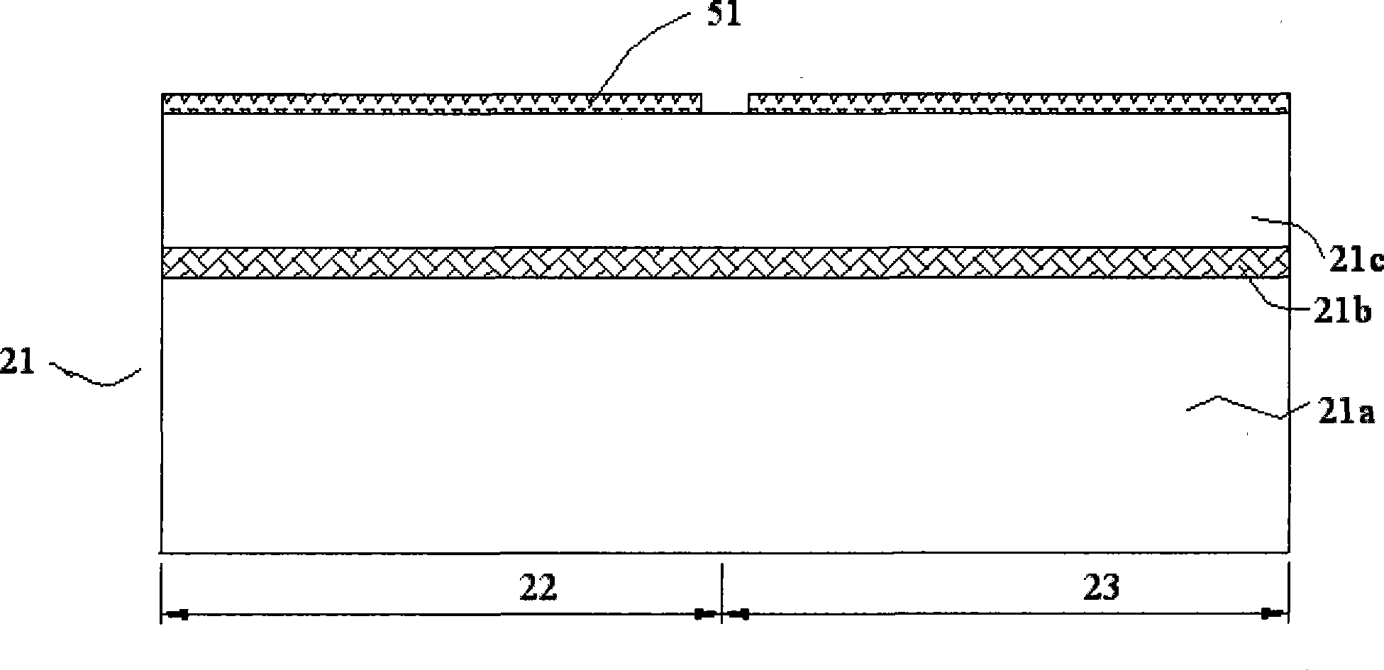
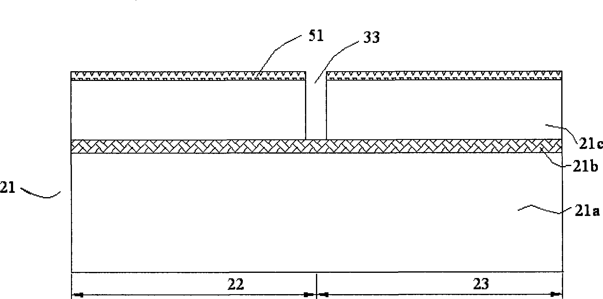
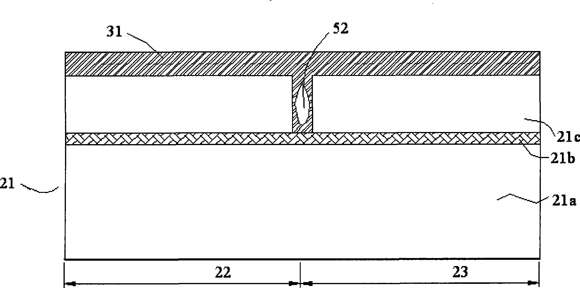
[0030] see Figures 1A-1E , the method for forming an electrical isolation region using a low-temperature process on an insulating silicon substrate may include the following steps:

[0031] First, if Figure 1A and Figure 1B As shown, according to the design requirements, the corresponding part of the device layer 21c of a silicon-on-insulator (SOI) substrate 21 is etched by deep groove reactive ion etching method or plasma dry etching method, and the etching is carried out to the silicon-insulator substrate. The silicon oxide buried layer 21b (between the device layer 21c and the substrate 21a of the insulating silicon substrate 21) that the sheet 21 has is used to form the corresponding isolation groove 33, and the insulating silicon substrate 21 is covered by the isolation groove 33 is divided into electrical isolation regions 22 and 23. For example, a mask layer 51 for deep groove reactive ion etching (DRIE) is usually formed on the device layer 21c first. This layer ca...

Embodiment 2

[0036] See Figure 2A-2E , the method for forming an electrical isolation region on an insulating silicon substrate using a low-temperature process may also include the following steps:

[0037] First, if Figure 2A As shown, according to design requirements, wet etching is used to etch the corresponding part of the device layer 21c that an insulating silicon substrate 21 has, and the etching is carried out to the silicon oxide buried layer 21b (in the insulating silicon substrate 21) that the insulating silicon substrate 21 has. between the device layer 21c of the silicon substrate 21 and the substrate 21a) to form a corresponding isolation groove 33, while the insulating silicon substrate 21 is separated into electrical isolation regions 22 and 23 by the isolation groove, for example, prior to the device A mask layer 61 for wet etching is formed on the layer 21c, and this layer can be a photoresist, or be deposited by a low temperature (less than 400°C) process (less than 4...


PUM


Abstract

A method of forming electrical isolated areas by adopting low temperature technology, a monolithic integrated process and a chip are provided. The integration of MEMS and an integrated circuit component can be realized through firstly etching relevant part of a component layer of an insulating silicon chip through adopting the wet etching, the plasma dry etching or the deep-slot ion etching method to form relative isolated grooves, separating the chip into a plurality of electrical isolated areas by the isolated grooves, then generating an insulating dielectric layer on the component layer through adopting the lower-temperature process under 400 DEG C, leveling the surface of the insulating dielectric layer on the isolated grooves, then forming relative connecting holes on the relative position of the insulating dielectric layer of each electric isolated area which requires the electric connection through adopting the wet etching or the dry etching, finally depositing a metal layer on the insulating dielectric layer, and forming a metal connecting wire which can metallically and mutually connect the connecting holes after the necessary etching, thereby realizing the necessary electric connection of relative electric isolated areas.

Description

technical field [0001] The present invention relates to a method for forming an electrical isolation region by using a low-temperature process on an insulating silicon substrate (SOI), and a method for monolithically integrating a micro-electromechanical device and an integrated circuit device by using a low-temperature process to form an electrical isolation region on an insulating silicon substrate , and monolithic integrated chips of micro-electromechanical devices and integrated circuit devices formed by forming electrical isolation regions on insulating silicon substrates by low-temperature technology. Background technique [0002] Micro-Electro-Mechanical System (MEMS) is a high-tech developed rapidly in recent years. It adopts advanced semiconductor preparation technology to realize the batch preparation of MEMS devices. Compared with traditional manufacturing technologies, devices made with MEMS technology have obvious advantages in terms of volume, power consumption...

Claims


Application Information

Patent Timeline
Patent Type & Authority Applications(China)
IPC IPC(8): H01L21/84H01L21/76H01L21/768H01L27/12H01L23/522B81C1/00B81B7/02
CPCH01L2924/0002
Inventor 李刚胡维
Owner MEMSENSING MICROSYST SUZHOU CHINA
Why Eureka
Try Eureka