Preparation for semi-conductor ferrous disilicide thin-film material

A technology of iron disilicide and thin film materials, which is applied in the field of preparation of β-FeSi2 thin films, and can solve the problems of impractical solar cells

Inactive Publication Date: 2009-03-18
NANJING UNIV OF AERONAUTICS & ASTRONAUTICS
View PDF0 Cites 0 Cited by
  • Summary
  • Abstract
  • Description
  • Claims
  • Application Information

AI Technical Summary

Problems solved by technology

But both teams used single-crystal Si substrates for the growth of semiconducting iron disilic...

Method used


Image

  • Preparation for semi-conductor ferrous disilicide thin-film material

Examples


no. 1 example

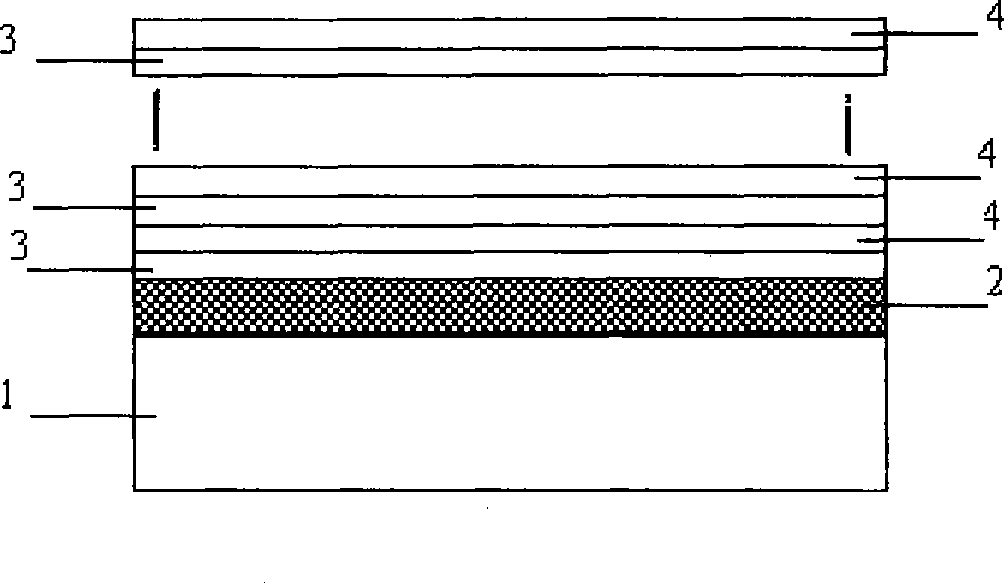
[0013] First Example: Using Surface Polished Al 2 o 3 The ceramic sheet is used as the substrate. After cleaning by the standard RCA process, it is placed in the magnetron sputtering chamber. The background vacuum is better than 5×10 -5 Pa, the vacuum of the deposition chamber is 0.1 Pa, and the purity of the Fe target and the Si target are 99.99% and 99.9999%, respectively. First deposit a layer of 25nm amorphous silicon film at room temperature, and then deposit 60 cycles of [Si3.3nm / Fe ​​1nm] multilayer film at room temperature. After annealing at 900°C for 2 hours in Ar gas atmosphere, the β-FeSi with preferred orientation of (202) was obtained 2 The thin film has a direct bandgap of 0.88eV; a resistivity of about 100Ω·cm, and weak n-type conductivity; and a photoconductive effect greater than 30% when irradiated by a 60W light source.

no. 2 example

[0014] The second embodiment: In the first embodiment, the conventional thermal annealing is changed to rapid thermal annealing, and the specific condition is to anneal at 1000°C for 15 seconds in an Ar gas atmosphere to obtain β-FeSi with a preferred orientation of (202) 2 The thin film has a direct bandgap of 0.87eV; a resistivity of about 120Ω·cm, and weak n-type conduction; when irradiated by a 60W light source, the photoconductive effect is about 35%.

no. 3 example

[0015] The third embodiment: In the first embodiment, the multilayer film structure is changed to [Si 3.3nm / Fe ​​1.6nm], and after annealing at 900°C for 2 hours in an Ar gas atmosphere, the β of the (202) preferred orientation is obtained. -FeSi 2 The thin film has a direct bandgap of about 0.88eV; a resistivity of about 0.3Ω·cm, and is p-type conductive.


PUM

PropertyMeasurementUnit
Thicknessaaaaaaaaaa
Thicknessaaaaaaaaaa
Resistivityaaaaaaaaaa

Abstract

A process for preparation of semiconductor ferrum disilicide film material relates to the process for preparing crystalline semiconducting phase ferrum disilicide (Beta-FeSi2) photoelectric films, which comprises the flowing steps: firstly cleaning a non-silicon substrate, secondly growing a silicon based transitional layer through the physical vapor deposition method, and finally depositing a multi-layer film through the physical vapor deposition method which specifically comprises depositing Fe thin layer with 0.5nm-5nm thickness and Si thin layer with 0.5nm-5nm thickness, wherein the thickness ratio of the Si thin layer and the Fe thin layer is within 1.8-3.6, the periodic time of the deposited Si/Fe multi-layer film is 1-200, the final step can be carried out under heating, or is carried out under the ambient temperature but needing the quenching treatment. The invention is a process for preparing the Beta-FeSi2 photoelectric film with controllable forbidden band width, crystal orientation and conductive types on a cheap non-silicon substrate, which has wide application and spread prospects.

Description

technical field [0001] The present invention relates to crystalline semiconductor phase iron disilicide (β-FeSi 2 ) Preparation method of photoelectric thin film, especially related to β-FeSi used in photoelectric devices 2 The method of film preparation, Background technique [0002] Today, as the world's oil resources are increasingly depleted, human beings have increased their efforts to find and utilize renewable energy. Among renewable energy sources, solar energy is the cleanest and most abundant energy resource bestowed by nature. In recent years, the photovoltaic industry around the world has developed rapidly. In terms of solar cells, it has gone through the "first generation" solar cells based on silicon wafers to the low-cost "second generation" thin-film solar cells, and now it has begun Develop "third generation" thin-film solar cells with high conversion efficiency, and stacked silicon-based thin-film solar cells are representatives of "third-generation" sol...

Claims


Application Information

Patent Timeline
IPC IPC(8): H01L31/18
CPCY02P70/50
Inventor 沈鸿烈鲁林峰尹玉刚
Owner NANJING UNIV OF AERONAUTICS & ASTRONAUTICS
Why Eureka
Try Eureka