Highly efficient LED having current spread layer construction improved and manufacturing method thereof

A current spreading layer, light emitting diode technology, applied in circuits, electrical components, semiconductor devices, etc., can solve problems affecting current spreading, increase in mesh dislocation density, device reliability and stability, and improve reliability. and stability, forward voltage reduction, and extension efficiency enhancement effects

Active Publication Date: 2009-03-18
XIAMEN CHANGELIGHT CO LTD
View PDF0 Cites 22 Cited by
  • Summary
  • Abstract
  • Description
  • Claims
  • Application Information

AI Technical Summary

Problems solved by technology

GaP material has good chemical stability, high electrical conductivity and full transparency to AlGaInP luminous wavelength. As a light-transmitting window, it can obtain high external quantum efficiency, but GaP material has a large lattice mismatch compared with AlGaInP material, reaching -3.6%, this mismatch leads to an increase in the network dislocation density formed at the interface, which is not conducive to the growth of GaP materials on AlGaInP materials, poor lattice quality at the interface, and low electron mobility, which not only affects the expansion of the current, but also It is easy to cause reliability and stability problems of the device
Al x Ga 1-x As the material of the current spreading layer, As material itself matches the lattice of AlGaInP material, can be heavily doped by P type and has high carrier mobility, but Al x Ga 1-x Since the As material contains aluminum components, the aluminum in the current spreading layer is easy to react with oxygen, water, etc. and deteriorate, which affects the reliability of the device.

Method used


Image

  • Highly efficient LED having current spread layer construction improved and manufacturing method thereof
  • Highly efficient LED having current spread layer construction improved and manufacturing method thereof
  • Highly efficient LED having current spread layer construction improved and manufacturing method thereof

Examples


Embodiment Construction

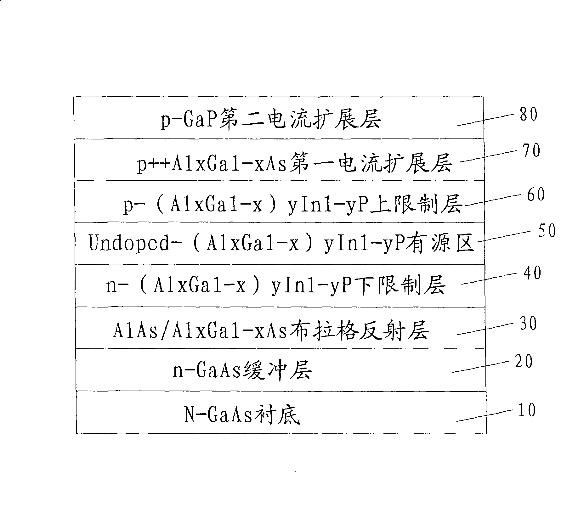
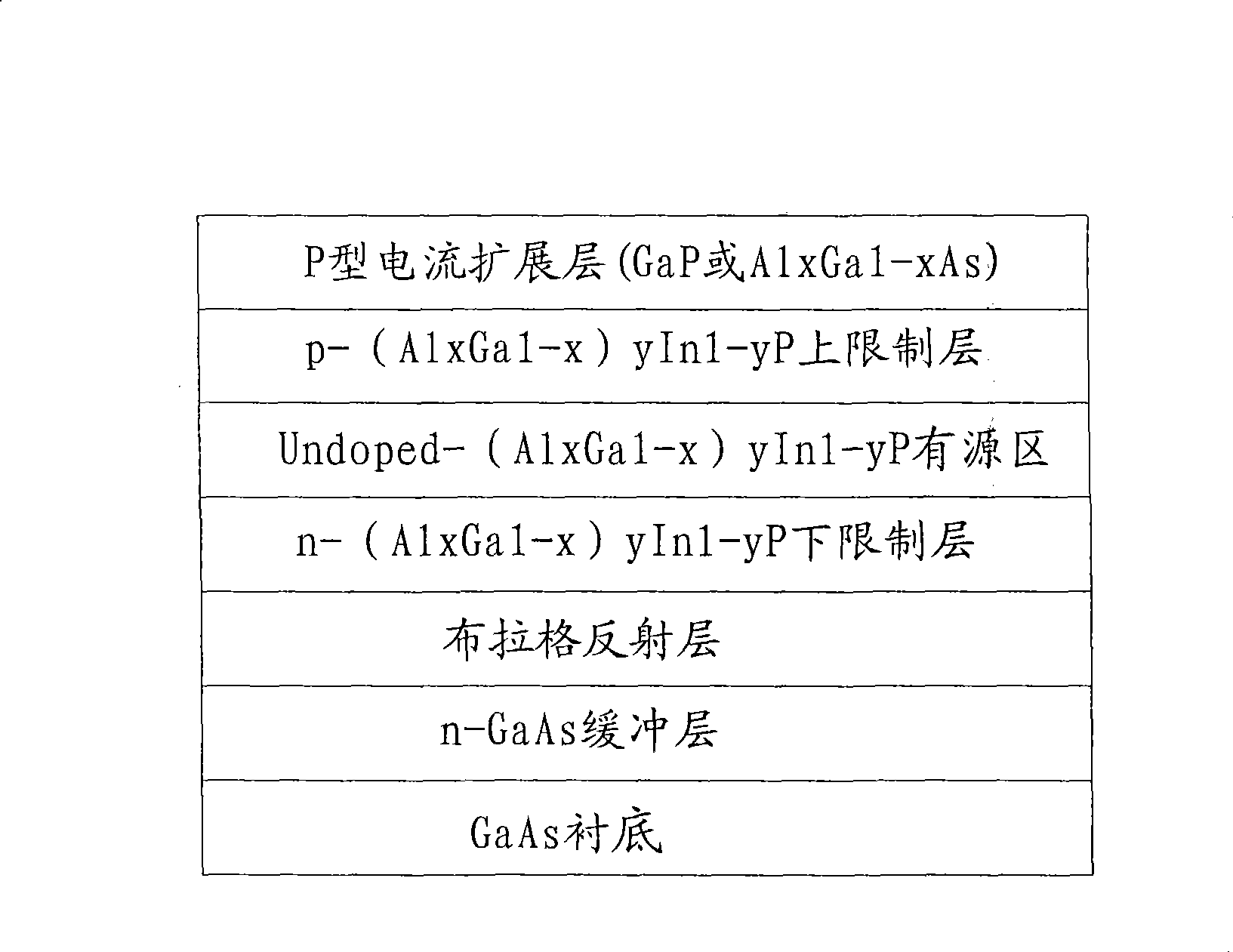
[0019] Such as figure 1 As shown, the AlGaInP light-emitting diode with the improved current spreading layer of the present invention is similar to the existing AlGaInP light-emitting diode in terms of epitaxial material structure. The epitaxial materials of the N-GaAs substrate 10 are: n-GaAs buffer layer 20, Bragg reflection layer 30, n-(Al x Ga 1-x ) y In 1-y P lower confinement layer 40, Undoped-(Al x Ga 1-x ) y In 1-y P active region 50, p-(Al x Ga 1-x ) y In 1-y Confinement layer 60 on P, p++Al x Ga 1-x As 70 and p-GaP 80 combined current spreading layer.

[0020] Wherein, the Bragg reflection layer 30 is AlAs / Al x Ga 1-x As or AlInP / (Al x Ga 1-x ) y In 1-y P, 0.35≤x≤0.7, period is 0~26, n-(Al x Ga 1-x ) y In 1-y In the P lower confinement layer 40, 0.6≤x≤1, 0.45≤y≤0.55, p-(Al x Ga 1-x ) y In 1-y In the P upper confinement layer 60, 0.6≤x≤1, 0.45≤y≤0.55, Undoped-(Al x Ga 1-x ) y In 1-yThe P active region 50 has an MQW (Multiple Quantum Hyd...


PUM


Abstract

The invention discloses a highly-effective light-emitting diode with an improved current spreading layer structure and a production method thereof. Material which is extended on an N-GaAs under-layer comprises an n-GaAs buffer layer, or an AlAs/AlxGal-xAs or AlInP/(A1x Ga1-x)yIn1-yP Bragg reflection layer, an n-(AlxGa1-x)yIn1-yP lower limiting layer, an Undoped-(AlxGa1-x)yIn1-yP active region, a p-(A1xGa1-x)yIn1-yP upper limiting layer, and a p++AlxGal-xAs and p-GaP combined current spreading layer, wherein the p++AlxGal-xAs is arranged on the lower surface as a first current spreading layer, and the p-GaP is arranged on the upper surface as a second current spreading layer. The structure integrates the advantages of GaP and A1xGal-xAs materials, avoids the oxidization of materials, and guarantees the reliability and the stability of the current spreading and apparatuses.

Description

technical field [0001] The invention belongs to the technical field of semiconductor devices, and relates to a high-efficiency light-emitting diode with an improved current spreading layer structure and a manufacturing method thereof. technical background [0002] Light-emitting diodes (LEDs) have the advantages of small size, solidification, long life, and low power consumption, which are incomparable to other types of display devices. In recent years, LED has jumped to the absolute dominant position of semiconductor optoelectronic devices in terms of output and output value, which is more than the sum of other semiconductor materials. [0003] Aluminum gallium indium phosphide AlGaInP light-emitting diode LED has excellent performance in yellow-green, orange, orange-red, and red bands. It has broad application prospects in chemical engineering and other fields. Epitaxial AlGaInP materials on gallium arsenide GaAs substrates can obtain light-emitting diodes with color cov...

Claims


Application Information

Patent Timeline
Patent Type & Authority Applications(China)
IPC IPC(8): H01L33/00H01L33/14
Inventor 蔡建九张银桥张双翔王向武
Owner XIAMEN CHANGELIGHT CO LTD
Why Eureka
Try Eureka