Distribution of current blocking layer, LED corresponding to the upper electrode and preparation thereof

A technology of current blocking layer and light emitting diode, which is applied to circuits, electrical components, semiconductor devices, etc., can solve the problems of weak lateral current expansion capability of the current expansion layer, low device luminous efficiency, poor thermal characteristics, etc., so as to improve light extraction. Efficiency and luminous intensity, simple process, effect of reducing thickness

Inactive Publication Date: 2009-03-18
沈光地
View PDF0 Cites 13 Cited by
  • Summary
  • Abstract
  • Description
  • Claims
  • Application Information

AI Technical Summary

Problems solved by technology

[0002] At present, the structure of ordinary light-emitting diodes such as figure 1 Shown: the upper electrode 10 has a diameter of 80-100 μm and a thickness of about Above the circular metal layer, current is injected from the electrode, and the photons generated are emitted from this side of the LED; the lower electrode 20 is the size of the entire surface of the LED device, with a thickness of about Above the metal layer, the main problem of the LED with this structure is: the current injected from the upper electrode 10 passes through the lateral expansion of the current spreading layer 100 and flows through the active region 200 to radiate and recombine to generate photons. Because the current epitaxial growth technology is difficult Obtaining a highly doped and thick current spreading layer results in a weak lateral current spreading ability of the current spreading layer. Therefore, most of the current injected from the upper electrode 10 is collected directly below the upper electrode 10, for example: for the front For an AlGaInP-based red LED with a chip size of 300 μm*300 μm, an 8 μm GaP current spreading layer is epitaxially grown by MOCVD (Metal Organic Chemical Vapor Deposition). If the diameter of the upper electrode 10 is 100 μm, it can be known by calculation that: The current accounts for more than 40% of the total injected current
Part of the current will still be collected directly under the upper electrode 10, even greater than the current collected under the bonding pad (see the ratio of the area of ​​the graphic electrode to the area of ​​the bonding pad), and the photons generated by this part of the current in the active region 200 will still be absorbed The blocking or absorption of the electrode 10 turns into a large amount of heat, resulting in problems such as low light efficiency, low brightness, and poor thermal characteristics of the device.

Method used


Image

  • Distribution of current blocking layer, LED corresponding to the upper electrode and preparation thereof
  • Distribution of current blocking layer, LED corresponding to the upper electrode and preparation thereof
  • Distribution of current blocking layer, LED corresponding to the upper electrode and preparation thereof

Examples


Embodiment 1

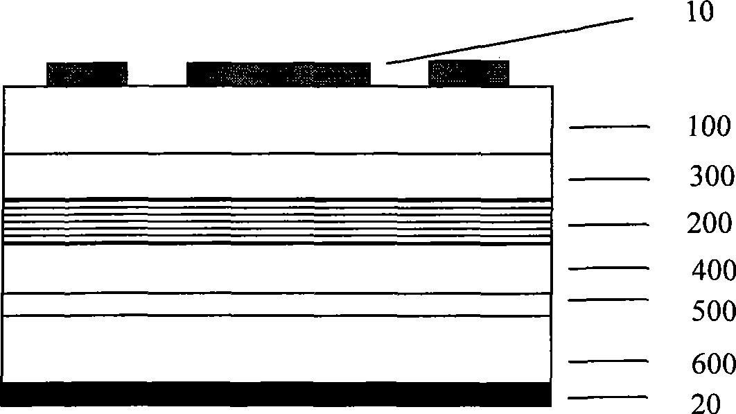
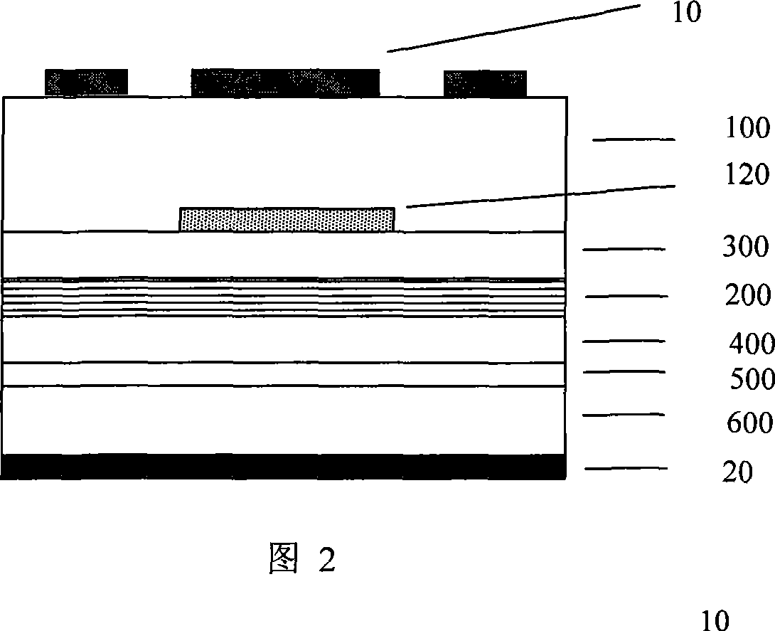
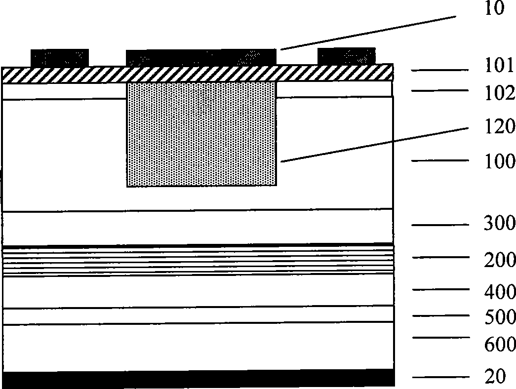
[0033] Such as Figure 7 As shown, take AlGaInP LED as an example. The device consists of the following parts: an upper electrode 10, a conductive optical anti-reflection layer 101, a current spreading layer 100, an upper confinement layer 300, an active region 200, a lower confinement layer 400, a buffer layer 500, a substrate 600, and a lower electrode 20 , the current blocking layer 120 is located inside the upper confinement layer 300 and the active region 200; its preparation process and method are as follows:

[0034]1. On the n-type substrate 600 formed by GaAs and other materials that can match AlGaInP, the buffer layer 500, the lower confinement layer 400, the active region 200, the upper confinement layer 300, and the current spreading layer 100 are epitaxially grown in sequence by MOVCD method , so that the epitaxial wafer of AlGaInP light-emitting diode is obtained;

[0035] 2. Then through the post-processing method: firstly, the epitaxial wafer is cleaned, the ...

Embodiment 2

[0038] In the present invention, the distribution of the current blocking layer corresponds to the light-emitting diode of the upper electrode, such as Figure 7 shown, where:

[0039] 1. In the present invention, the shape of the upper electrode 10 can be circular, star-shaped, strip-shaped, finger-shaped or other shapes, and the diameter of the welding spot can be 100 μm, 80 μm or other sizes.

[0040] 2. The material of the current blocking layer 120 can be an insulating material such as an intrinsic semiconductor, a non-conductive resin, non-doped amorphous Si, SixNy and SixOy, or a conductive material opposite to the conductive type of the conductive optical anti-reflection layer 101;

[0041] 3. The structure of the active region 200 is a p-n junction, or a p-i-n junction, or a double heterostructure, or a single quantum well structure, or a multi-quantum well structure, a superlattice structure, or a quantum dot light-emitting structure, or a multilayer quantum dot stru...


PUM


Abstract

The invention relates to the distribution of a current barrier layer, a light-emitting diode which is corresponding to an upper electrode and a process for preparation, belonging to the technical field of semiconductor photoelectrons. The structure comprises an upper electrode (10), a current spreading layer (100), an upper limiting layer (300), an active region (200), a lower limiting layer (400), a buffer layer (500), an under-layer (600) and a lower electrode (20), and further comprises a current barrier layer (120) located on the right lower portion of the upper electrode, wherein the distribution of the current barrier layer is corresponding to the upper electrode, a conductive light anti-reflection layer (101) is arranged between the upper electrode and the current spreading layer inside the conductive light anti-reflection layer or the current spreading layer or the upper limiting layer or the active region, or inside adjacent two layers, three layers or four layers, wherein the current barrier layer is realized through the post techniques. The current barrier layer corresponding to the upper electrode nearly completely avoids light and heat loss generated by idle current, thereby increasing the light extraction efficiency of the LED, and increasing the light emitting intensity, and the structure reduces the generation of heat, which is especially suitable for the preparation of large-power LEDs.

Description

technical field [0001] The light-emitting diode with the distribution of the current blocking layer corresponding to the upper electrode and the preparation method thereof relate to a novel LED device structure and belong to the technical field of semiconductor optoelectronics. Background technique [0002] At present, the structure of ordinary light-emitting diodes such as figure 1 Shown: the upper electrode 10 has a diameter of 80-100 μm and a thickness of about Above the circular metal layer, current is injected from the electrode, and the photons generated are emitted from this side of the LED; the lower electrode 20 is the size of the entire surface of the LED device, with a thickness of about Above the metal layer, the main problem of the LED with this structure is: the current injected from the upper electrode 10 passes through the lateral expansion of the current spreading layer 100 and flows through the active region 200 to radiate and recombine to generate photo...

Claims


Application Information

Patent Timeline
Patent Type & Authority Applications(China)
IPC IPC(8): H01L33/00
CPCH01L33/145H01L33/44
Inventor 沈光地陈依新
Owner 沈光地
Why Eureka
Try Eureka