Method for making near infrared band three-dimensional photon crystal

A photonic crystal, near-infrared technology, applied in the directions of light guide, optics, optical components, etc., can solve the problems of three-dimensional photonic crystal difficulty, and achieve the effect of high precision and insensitive card installation stability.

Active Publication Date: 2009-03-25
SUZHOU UNIV
View PDF0 Cites 10 Cited by
  • Summary
  • Abstract
  • Description
  • Claims
  • Application Information

AI Technical Summary

Problems solved by technology

Due to the problems in the above technical solutions, it is still very difficult to make three-dimensional photonic crystals in the near-infrared band in the field of visible light and optical communication.

Method used


Image

  • Method for making near infrared band three-dimensional photon crystal
  • Method for making near infrared band three-dimensional photon crystal
  • Method for making near infrared band three-dimensional photon crystal

Examples


Embodiment 1

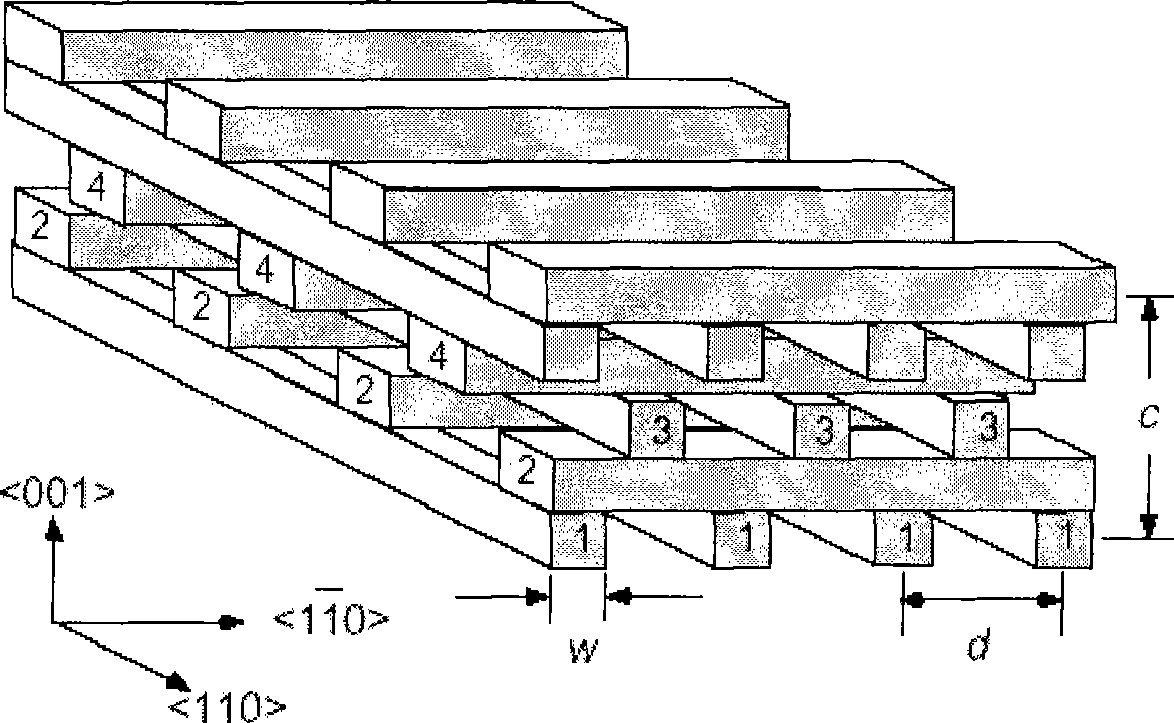
[0055] Embodiment 1: A method for making a three-dimensional photonic crystal in the near-infrared band, which is implemented by layer-by-layer superposition method, comprising the following steps:

[0056] (1) Deposit a silicon dioxide layer on a silicon substrate by ECR-CVD method, and control the thickness to be 0.2 microns;

[0057] (2) Coating photoresist, using holographic photolithography to make a photoresist mask on the photoresist, the period (d) of the one-dimensional grating structure obtained is 0.7 microns; the duty ratio (w / d) is 0.4;

[0058] (3) Reactive ion beam etching is used to realize mask transfer, and grooves are formed on the silicon dioxide layer. In this embodiment, trifluoromethane reactive ion beam etching is used, with ion energy of 390ev, ion beam current of 90mA, and accelerating voltage 270v, working pressure 1.3×10 -2 Pa;

[0059] (4) ECR-CVD method is used to fill the etched trench with high refractive index material silicon;

[0060] (5)...

Embodiment 2

[0075] Embodiment 2: A method for making a three-dimensional photonic crystal in the near-infrared band, which is realized by layer-by-layer superposition method, comprising the following steps:

[0076] (1) Deposit a silicon dioxide layer on a silicon substrate by ECR-CVD method, and control the thickness to be 0.2 microns;

[0077] (2) Coating photoresist, using holographic photolithography to make a photoresist mask on the photoresist, the period (d) of the one-dimensional grating structure obtained is 0.7 microns; the duty ratio (w / d) is 0.35;

[0078] (3) Reactive ion beam etching is used to realize mask transfer, and grooves are formed on the silicon dioxide layer. In this embodiment, trifluoromethane reactive ion beam etching is used, with ion energy of 390ev, ion beam current of 90mA, and accelerating voltage 270v, working pressure 1.3×10 -2 Pa;

[0079] (4) One side edge of the silicon substrate is set as the first reference grating area, and the ECR-CVD method is ...


PUM


Abstract

The invention discloses a method for manufacturing a near infrared waveband three-dimensional photonic crystal, wherein an one-dimensional crystal mask is formed by utilization of holographic interference, and is transferred onto a SiO2 layer on a silicon substrate material through ion beam etching or reactive ion beam etching; high refractive index materials are filled into an etched groove; the surface is polished by the ion beam etching method, and then SiO2 is deposited; a second layer is formed after coating of photoresist, holographic photoetching, ion beam etching and so on; the steps are repeated, and layers are aligned by the Moire fringe technique; and finally the SiO2 is removed by the acid washing method, and the three-dimensional photonic crystal required is obtained. The method fully utilizes the submicron resolution of holographic photoetching, can manufacture the large-area three-dimensional photonic crystal which can then be cut into small blocks as required, has the advantages of high efficiency and low cost, and simultaneously is convenient to overcome the defects of introduction of large area and periodicity by changing wave fronts of two beams of coherent light in an interference field.

Description

technical field [0001] The invention relates to a method for manufacturing a photonic crystal, in particular to a method for manufacturing a three-dimensional photonic crystal for near-infrared bands realized by holography-ion beam etching. Background technique [0002] The microelectronics revolution represented by the large-scale application of semiconductor technology in the 1950s brought mankind into a rapidly developing electronic age. However, with the development and progress of the times, the further integration of electronic devices at the nanoscale has become more and more difficult, and the resulting huge energy consumption has also become more and more difficult to influence the device's operating speed and performance improvement. Overcome, thus forming the so-called "electronic bottleneck" puzzlement. Photonic devices based on photon motion bring people hope to solve the problem. Compared to electrons, photons are much faster and have little interaction. The...

Claims


Application Information

Patent Timeline
Patent Type & Authority Applications(China)
IPC IPC(8): G02B6/122G03F7/00G03F7/36G03F7/42
Inventor 刘全吴建宏辛煜陈新荣李朝明胡祖元
Owner SUZHOU UNIV
Why Eureka
Try Eureka