Manufacturing method for gate lateral wall layer and semi-conductor device

A gate sidewall layer and gate sidewall technology, which is applied in semiconductor/solid-state device manufacturing, semiconductor devices, electrical components, etc. Bottom sag, leakage current and other problems, to reduce the probability of contamination, save time, and simplify process steps

Inactive Publication Date: 2009-03-25
SEMICON MFG INT (SHANGHAI) CORP
View PDF1 Cites 18 Cited by
  • Summary
  • Abstract
  • Description
  • Claims
  • Application Information

AI Technical Summary

Problems solved by technology

[0011] However, when the surface of the semiconductor substrate is subsequently cleaned with hydrofluoric acid (for example, when forming a metal silicide contact), the bottom of the gate sidewall layer will be recessed, such as image 3 The shown depression 14b, the depression 14b is caused by the corrosion of the silicon oxide layer 14a by hydrofluoric acid in the lateral direction
The recess 14b will shorten the conductive channel of the formed metal oxide semiconductor device, which will easily cause the problem of leakage current between the source and the drain.

Method used


Image

  • Manufacturing method for gate lateral wall layer and semi-conductor device
  • Manufacturing method for gate lateral wall layer and semi-conductor device
  • Manufacturing method for gate lateral wall layer and semi-conductor device

Examples


Embodiment Construction

[0080] The specific embodiments of the present invention will be described in detail below in conjunction with the accompanying drawings.

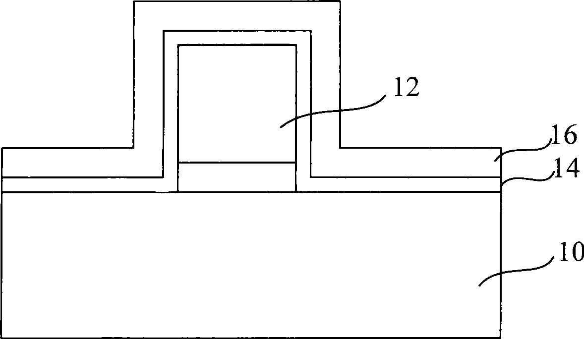
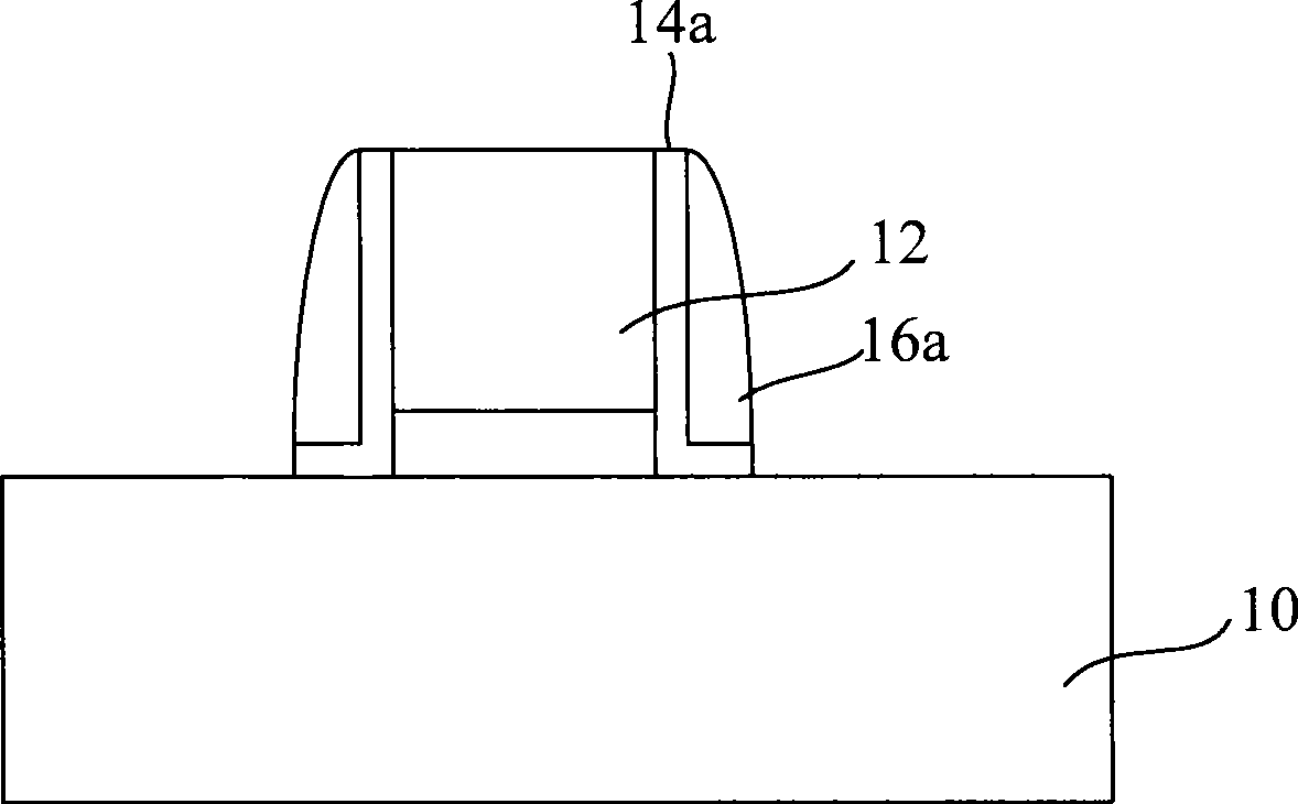
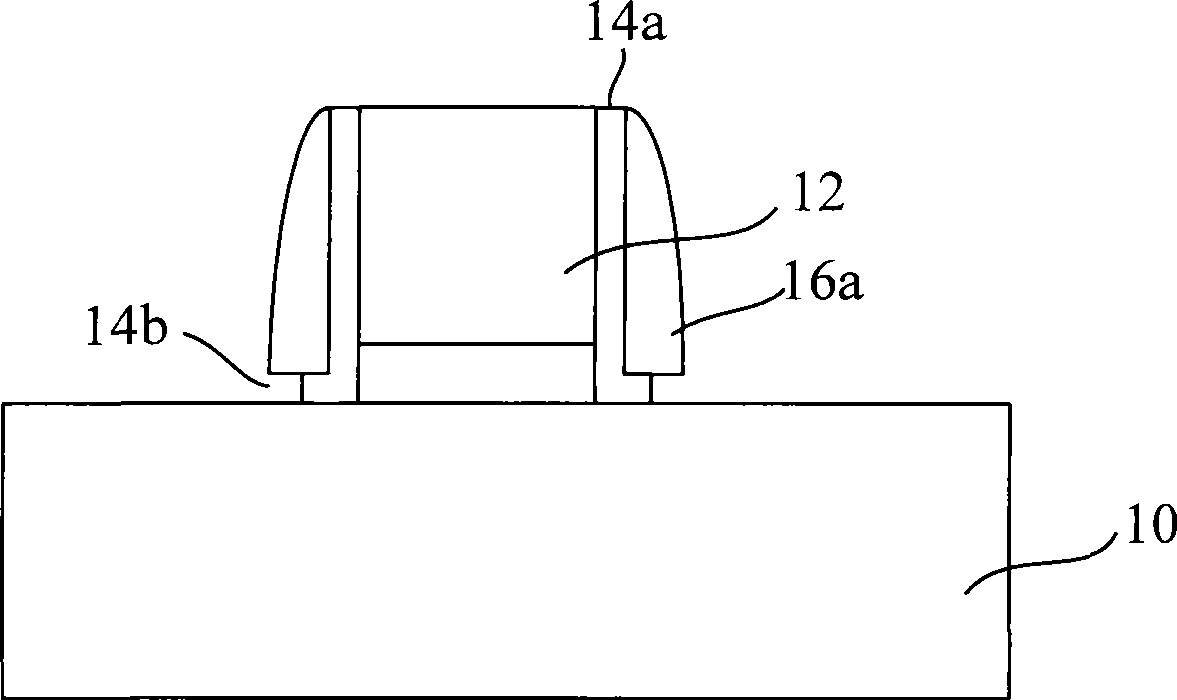
[0081] In the manufacturing process of the metal oxide semiconductor device, after the gate is formed, a gate sidewall layer needs to be formed on the sidewall of the gate to protect the formed gate. The present invention proposes a method for forming gate sidewall layers of a silicon oxide-silicon nitride (ON) structure or a silicon oxide-silicon nitride-silicon oxide (ONO) or multi-layer ON structure, which can improve or eliminate gate The bottom of the extreme sidewall layer is recessed, and the process is simple and the thermal budget is low, which helps to form a metal oxide semiconductor device with stable performance.

[0082] Figure 4 It is a flow chart of an embodiment of the method for forming the gate sidewall layer of the present invention. Figure 5 to Figure 10 A schematic cross-sectional structure diagram illustrating an...


PUM

PropertyMeasurementUnit
thicknessaaaaaaaaaa

Abstract

A method for forming a side wall layer on a grid electrode comprises the following steps: a semi-conductor substrate provided with the grid electrode is provided; a first silica layer is formed on the surfaces of the semi-conductor substrate and the grid electrode; with hexa-chloro silane as a precursor, a first silicon nitride layer is formed on top of the first silica layer; and parts of the first silica layer and the first silicon nitride layer are removed in a selective manner so as to preserve the first silica layer and the first silicon nitride layer already formed on the side wall of the grid electrode. The invention further provides a method for manufacturing a semiconductor device. The invention can solve the problem that the bottom part of the side wall layer on the grid electrode is susceptible to depression.

Description

technical field [0001] The invention relates to the technical field of semiconductor manufacturing, in particular to a method for manufacturing a gate sidewall layer (Sidewall Spacer) and a method for manufacturing a semiconductor device. Background technique [0002] Metal oxide semiconductor devices are widely used in storage, digital, computer, communication and other fields due to their high response rate and low power consumption. Generally, a metal oxide semiconductor device has a gate, a source and a drain, and the gate controls the on and off between the source and the drain. A gate sidewall layer is provided on the sidewall of the gate, and the gate sidewall layer is used to protect the gate and the conductive channel below the gate. The gate sidewall layer is generally composed of insulating silicon oxide or silicon nitride or a stack of both. [0003] At 0.18um and higher technology nodes, silicon oxide as the gate sidewall layer is generally formed by chemical ...

Claims


Application Information

Patent Timeline
Patent Type & Authority Applications(China)
IPC IPC(8): H01L21/28H01L21/31H01L21/316H01L21/318H01L21/311H01L21/336
Inventor 何有丰朴松源白杰唐兆云
Owner SEMICON MFG INT (SHANGHAI) CORP
Why Eureka
Try Eureka