Flatness-raised pixel electrode manufacture method

A technology for pixel electrodes and manufacturing methods, which is applied in the field of silicon-based liquid crystal manufacturing, can solve problems such as uneven thickness and inconsistency of liquid crystals, and achieve the effects of improved display contrast, improved performance, and improved thickness consistency

Active Publication Date: 2009-04-01
SEMICON MFG INT (SHANGHAI) CORP
View PDF0 Cites 1 Cited by
  • Summary
  • Abstract
  • Description
  • Claims
  • Application Information

AI Technical Summary

Problems solved by technology

[0004] However, after the above maskless etching step, the grid-shaped oxide also has a part protruding from the pixel electrode, see figure 1 , which shows a cross-sectional view of the silicon substrate 1 after maskless etching, as shown in the figure, the gate oxide 10 has a protrusion 100 higher than the pixel electrode 11, so when the silicon substrate with the protrusion 100 When the liquid crystal is filled on the substrate 1, the local irregularity of the liquid crystal arrangement and the inconsistency of the thickness will be caused.

Method used


Image

  • Flatness-raised pixel electrode manufacture method
  • Flatness-raised pixel electrode manufacture method
  • Flatness-raised pixel electrode manufacture method

Examples


Embodiment Construction

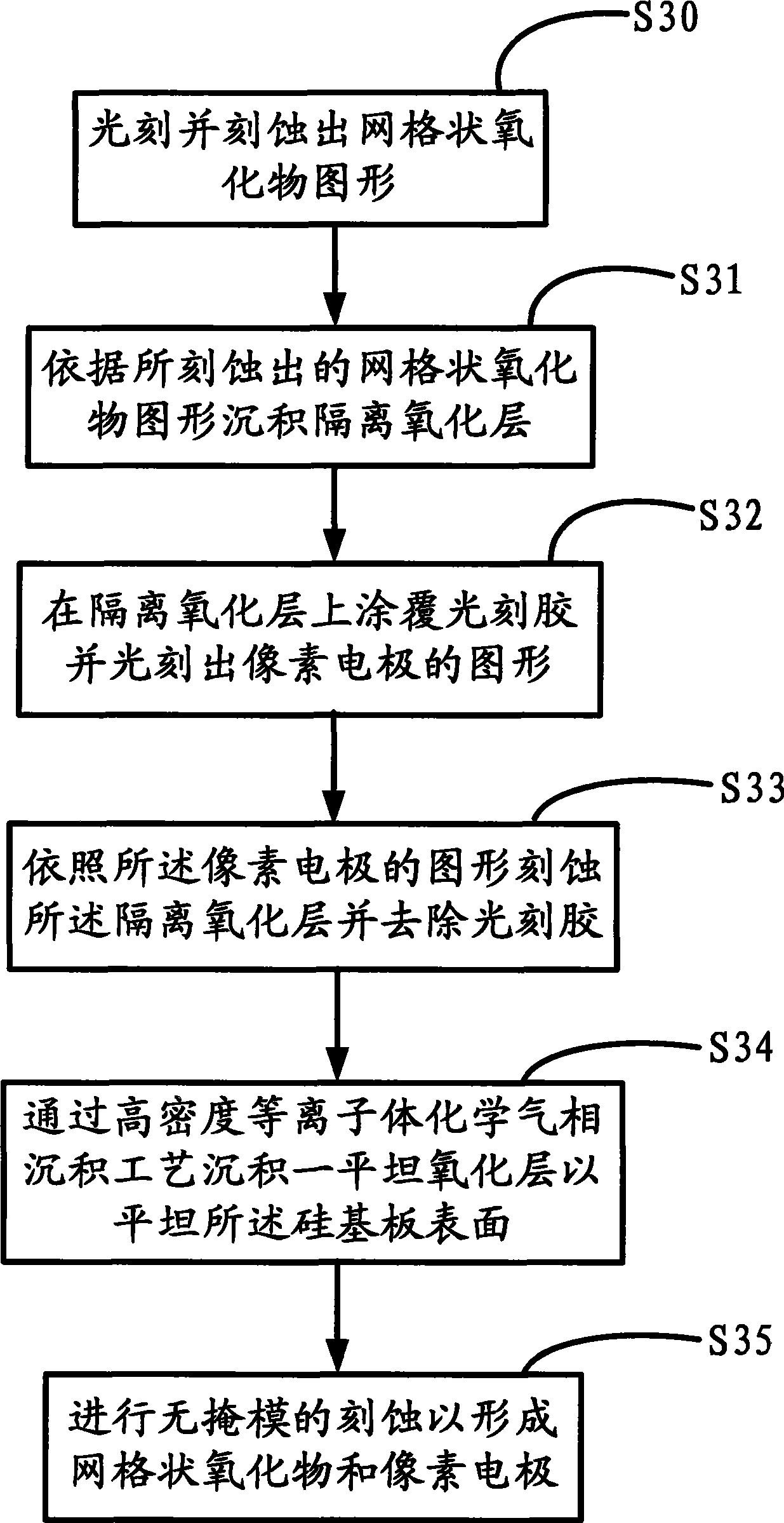
[0020] The method for manufacturing the pixel electrode that can improve the flatness of the present invention will be further described in detail below.

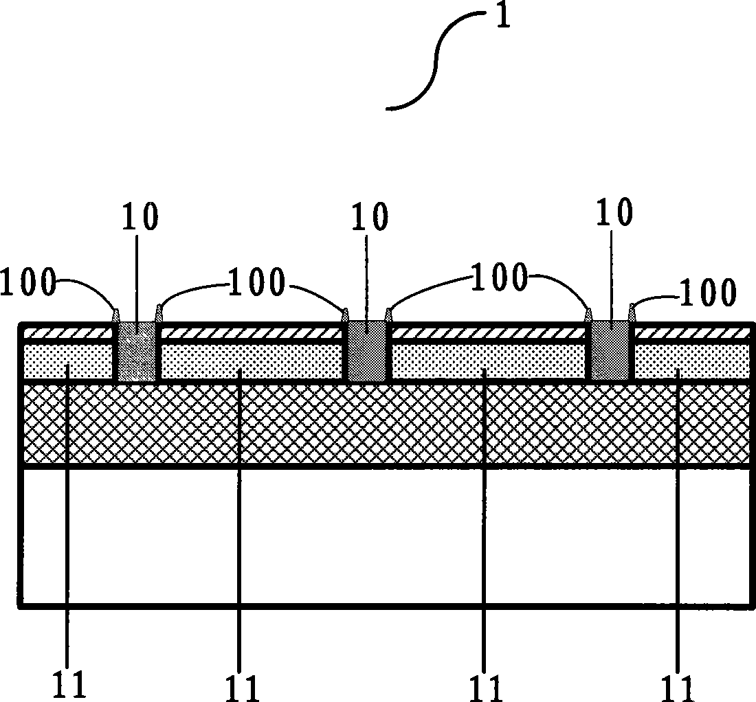
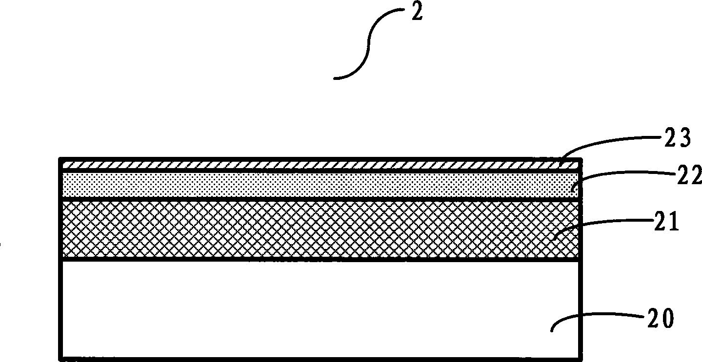
[0021] see figure 2 The pixel electrode in the pixel electrode manufacturing method that can improve the flatness of the present invention is fabricated on the silicon substrate 2, the silicon substrate 2 has a control circuit 20, and an interlayer insulating layer 21 stacked on the control circuit 20 in sequence , top metal layer 22 and protective oxide layer 23 . In this embodiment, the control circuit 20 is composed of MOS tubes, and the internal components of the control circuit 20 are not described in detail here, and the interlayer insulating layer 21 is made of borophosphosilicate glass (Boro-phospho-silicate glass). silicate Glass, BPSG), the top metal layer 22 is the fourth metal layer and it is aluminum, and the protective oxide layer 23 is made by atmospheric radio frequency cold plasma (TEOS) process.

[0022...


PUM


Abstract

The invention provides a pixel electrode preparation method which can improve the flatness, and the pixel electrode is manufactured on a silicon substrate which is provided with a control circuit, as well as top metal and a protective oxide layer which are stacked on the control circuit. In the prior art, when the pixel electrode is manufactured, latticed oxide is prone to be facilitated to generate a convex, thus affecting the flatness of the pixel electrode, and further affecting the performance of liquid crystal on the silicon substrate. In the pixel electrode preparation method, firstly, a latticed oxide pattern used for dividing the top metal into a plurality of pixel electrodes is prepared by lithography and etching; then, an isolation oxide layer is deposited; after that, optical resist is coated on the isolation oxide layer and a pattern of pixel electrodes is prepared by lithography; then, the isolation oxide layer is etched according to the pattern of pixel electrodes and the optical resist is removed; after that, a flat oxide layer is deposited on the flat surface of the silicon substrate; finally, maskless etching is carried out to form the latticed oxide and the pixel electrodes. The invention has the advantage that the flatness of the pixel electrode can be greatly improved, and then the performance, especially the display contrast, of the liquid crystal on the silicon substrate is improved.

Description

technical field [0001] The invention relates to the field of silicon-based liquid crystal manufacturing, in particular to a method for manufacturing pixel electrodes that can improve flatness. Background technique [0002] The structure of Liquid Crystal On Silicon (LCOS) is a sandwich structure, that is, the liquid crystal material is sandwiched between a transparent glass plate as a common electrode and a silicon substrate containing pixel electrodes and their control circuits. LCOS combines Combining semiconductor and liquid crystal technology, it has many advantages such as high density, high resolution, high resolution, high aperture ratio, power saving and low cost, so it has become the new mainstream of large-screen high-resolution and low-cost projection display technology. [0003] The ideal LCOS silicon substrate should be flat and smooth with high reflectivity, so as to ensure good liquid crystal alignment and consistency of liquid crystal layer thickness, and not...

Claims


Application Information

Patent Timeline
IPC IPC(8): H01L21/822H01L21/71G02F1/1362
Inventor 蒲贤勇陈轶群刘伟曾贤成
Owner SEMICON MFG INT (SHANGHAI) CORP
Why Eureka
Try Eureka