LDMOS chip light doped drift region structure and forming method

A lightly doped, drift region technology, applied in the fields of communication and radar, can solve the problems of low frequency gain of LDMOS devices, deterioration of device frequency and power characteristics, and total reduction of LDD impurities, so as to improve device breakdown voltage, Improved frequency and power performance, optimized positive ion distribution

Inactive Publication Date: 2010-08-25
BEIJING MXTRONICS CORP +1
View PDF0 Cites 0 Cited by
  • Summary
  • Abstract
  • Description
  • Claims
  • Application Information

AI Technical Summary

Problems solved by technology

However, the reduction of LDD doping concentration will lead to the reduction of the total amount of LDD impurities, which will cause the source-drain on-resistance to increase, resulting in a sharp decrease in the high-frequency gain of the LDMOS device, and the deterioration of the frequency and power characteristics of the device.
Therefore, reducing the drain resistance and increasing the breakdown voltage of the device are a pair of contradictions that are difficult to reconcile with conventional LDD structure LDMOS chips.

Method used


Image

  • LDMOS chip light doped drift region structure and forming method
  • LDMOS chip light doped drift region structure and forming method
  • LDMOS chip light doped drift region structure and forming method

Examples


Embodiment Construction

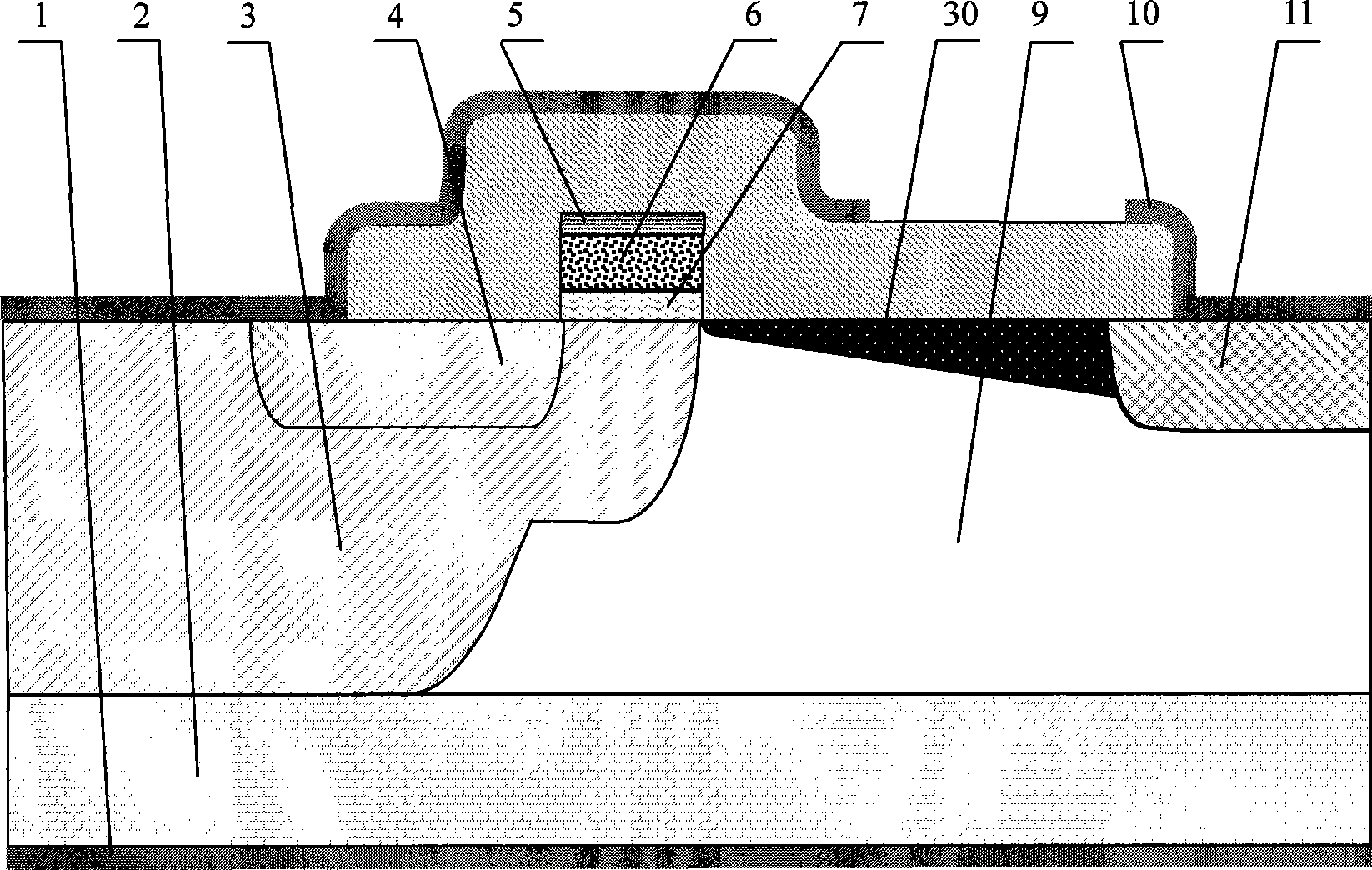
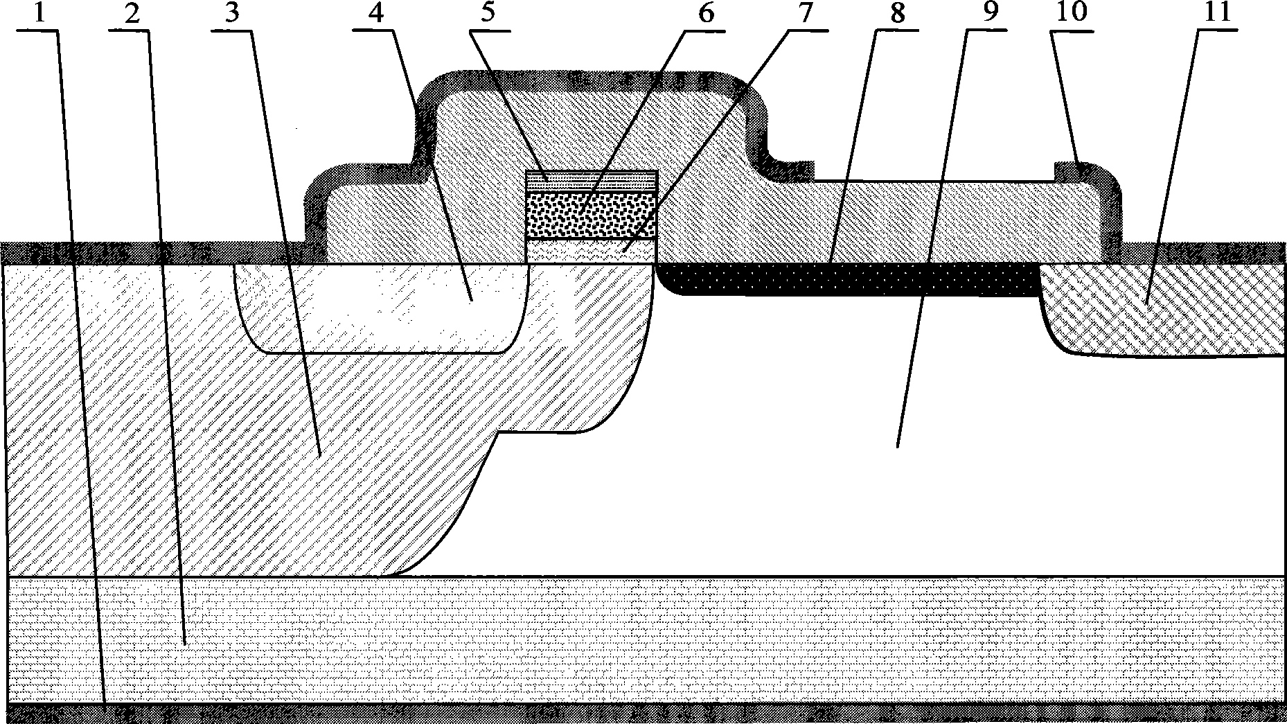
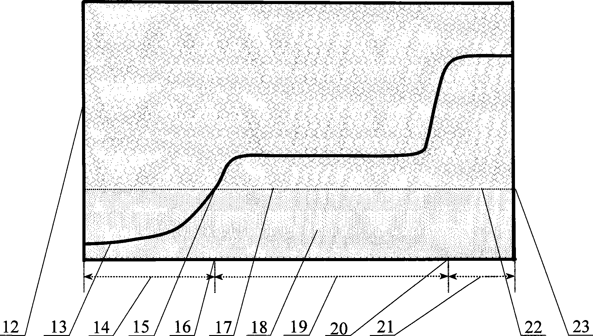
[0021] As shown in Figure 5, the structure of the present invention includes source 1, P+ substrate 2, P-type double diffusion region 3, N-type source region 4, metal silicide and gate 5, gate polysilicon 6, gate oxide 7, Conventional lightly doped drift region (LDD) 30, P-type epitaxy 9, drain 10, N-type drain 11, etc., P-type double diffusion region 3 forms a channel region under the gate oxide 7, and LDD 30 is located in the channel Between the channel region and the N-type drain region 11, the LDMOS chip structure of the present invention is characterized in that the LDD 30 formed between the channel region and the N-type drain region 11 has a non-uniform doping concentration, and the doping concentration is in the vertical direction (from the chip From the upper surface to the lower surface to the bottom of the censer) and laterally (the side close to the gate area to the side close to the drain area) simultaneously form a concentration gradient. As shown in Figure 6, 12 i...


PUM


Abstract

The invention relates to a lightly-doped drift region structure of an LDMOS chip and a formation method, a thin film layer is firstly covered on the upper surface of an LDD structure before the doping to form an LDD vicinal structure after being covered by the thin film layer, an ion injection barrier layer is formed at the LDD vicinal structure through the physical and chemical methods to further form the LDD structure before the doping, the thickness of the barrier layer is gradually reduced from one side which is near to a gate region to the other side which is near to a drain region, the ion injection of N-type impurities is finally carried out on the surface of the LDMOS chip device, and the LDD structure with the simultaneous approximate linear increase along vertical and horizontaldirections is finally formed. The LDD simultaneously forms the concentration gradients along the horizontal and the vertical directions, thereby leading the LDD doping concentration to be linearly increased from the side which is near to a gate to the side which is near to a drain; compared with the conventional LDMOS, the lightly-doped drift region structure can improve the device breakdown voltage under the situation of maintaining the resistance of the drain unchanged basically or greatly reducing the resistance of the drain at the same time of maintaining the device breakdown voltage unchanged basically, thereby improving the frequency and the power performance of the LDMOS device.

Description

Technical field [0001] The invention relates to a semiconductor chip structure, in particular to a new structure forming method of a lightly doped drift region of an LDMOS chip, which is mainly used in the fields of communication, radar and the like. Background technique [0002] Lateral double diffused metal oxide semiconductor (LDMOS) devices have a wide range of applications in communications, radar and other fields due to their many advantages. In order to obtain larger output power and higher reliability, it is usually required that the source and drain regions have a higher reverse breakdown voltage. The conventional method is to make a lightly doped drift region (LDD) on the side of the drain of the MOS transistor to reduce the doping concentration of the drain region and expand the width of the ionization layer to obtain a higher reverse breakdown voltage. [0003] Figure 1 shows the structure of a conventional LDMOS chip, including source 1, P+ substrate 2, P-type double ...

Claims


Application Information

Patent Timeline
Patent Type & Authority Patents(China)
IPC IPC(8): H01L29/78H01L29/06H01L21/336H01L21/265
CPCH01L29/7835H01L21/2652H01L29/0847H01L29/1045
Inventor 冯幼明王传敏
Owner BEIJING MXTRONICS CORP
Why Eureka
Try Eureka