
Ceramic laminated device and method for manufacturing same

A ceramic and multilayer technology, applied in the direction of multilayer capacitors, multilayer circuit manufacturing, printed circuit manufacturing, etc., can solve the problems of easy loss, lower device Q value, electrode width or thickness smaller than the design value, etc. Q value, excellent characteristics, and the effect of small variation in characteristics

Inactive Publication Date: 2009-04-01
PANASONIC CORP
View PDF2 Cites 6 Cited by
  • Summary
  • Abstract
  • Description
  • Claims
  • Application Information

AI Technical Summary

Problems solved by technology

[0006] However, in the above-mentioned conventional example, there is a problem that although sintering can be performed at a temperature of about 900° C. that can be sintered simultaneously with silver (Ag), when a ceramic laminated device is formed, the ceramic material is Reaction with silver (Ag) makes the electrode width or thickness smaller than the design value, and sufficient characteristics cannot be obtained
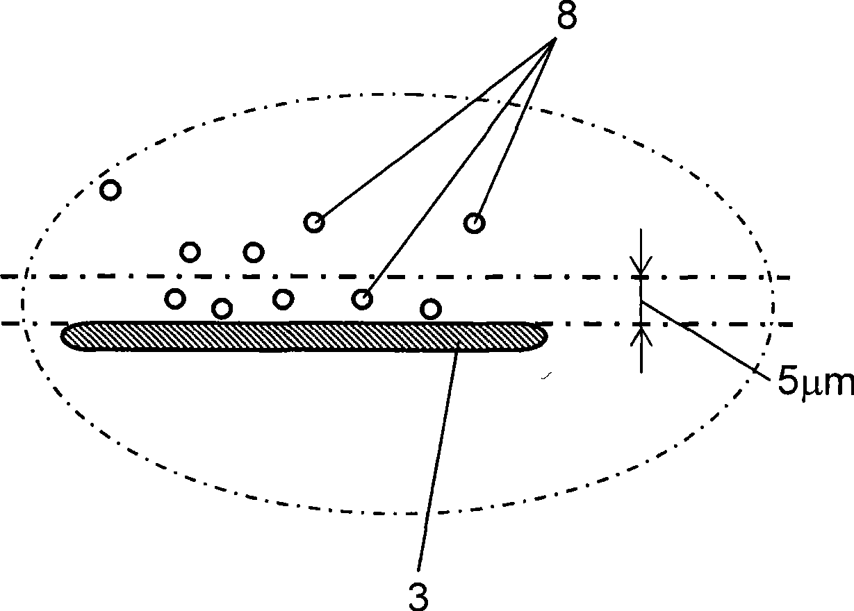
Furthermore, silicon (Si) or zinc (Zn), which is a component of glass or additives, or their composite oxides, etc., segregate as a secondary phase near the electrode, thereby reducing the Q value of the device and easily increasing the loss. The problem

Method used


Image

  • Ceramic laminated device and method for manufacturing same
  • Ceramic laminated device and method for manufacturing same
  • Ceramic laminated device and method for manufacturing same

Examples


Embodiment Construction

[0025] Hereinafter, a ceramic multilayer device and a manufacturing method according to one embodiment of the present invention will be described.

[0026] BaCO with high chemical purity (99% by weight or more) is used as the first component of the raw material 3 、Nd 2 o 3 、TiO 2 and Bi 2 o 3 . When xBaO-yNd 2 o 3 -zTiO 2 -wBi 2 o 3 When (x+y+z+w=100, x, y, z, and w are molar ratios) represent the composition of each component, the preferred composition range is 12≤x≤16, 12≤y≤16, 65≤z≤ 69. 2≤w≤5. In addition, although Nd is used here 2 o 3 As rare earth oxides, but oxides other than Nd such as La 2 o 3 、Sm 2 o 3 and other rare earth oxides. In addition, a part of Nd may be replaced with other rare earth elements. The above powder was mixed with pure water in a ball mill for 18 hours. After mixing, the slurry was dried, placed in an alumina crucible, and calcined at a temperature of 1200° C. to 1400° C. for 2 hours. The calcined powder was roughly pulverize...


PUM


Abstract

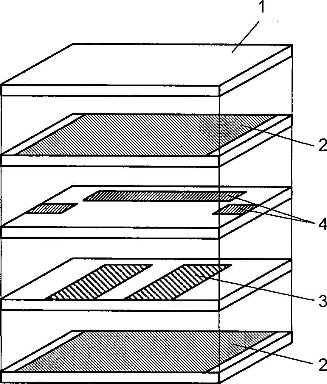
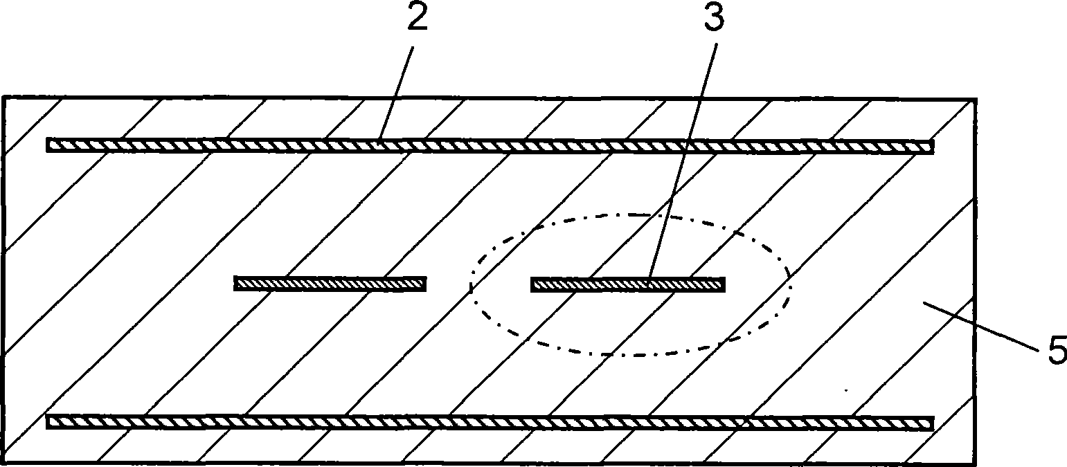
The present invention relates to a ceramic laminated device including a dielectric ceramic and an Ag electrode. In a dielectric ceramic that can be sintered at low temperatures and has a high dielectric constant and Q value, reactivity between the ceramic and Ag during sintering is suppressed low and segregation of specific elements in the proximity of the electrode is controlled. Thus, a filter having a high Q value and low loss is produced stably. For this purpose, in a ceramic laminated body including at least a ceramic and a Si-containing glass, a ratio of A / B, i.e. a ratio of a Si element concentration (A) within a range at a distance of 5 [mu]m or smaller from the Ag electrode to a Si element concentration (B) within a range at a distance larger than 5 [mu]m from the Ag electrode, is set equal to or smaller than 2.

Description

technical field [0001] The present invention relates to a ceramic laminated device and its manufacturing method. Background technique [0002] In recent years, with the development of communication technology using electromagnetic waves in the microwave region used in mobile phones, wireless local area networks (LANs), and the like, there has been an increasing demand for miniaturization of equipment. In order to realize miniaturization of these terminal devices, it is necessary to miniaturize high-frequency devices such as high-frequency filters and resonators constituting the devices. [0003] One of such high-frequency devices is a laminated dielectric filter. A laminated dielectric filter is formed by appropriately arranging internal electrodes (conductor metals) that form capacitors or striplines on the inner layer portion of a ceramic laminate made of dielectric ceramics, and utilizes the same resonant mode In the case of high-frequency components, the size of the hi...

Claims


Application Information

Patent Timeline
Patent Type & Authority Applications(China)
IPC IPC(8): H05K3/46
CPCH01G4/129H05K3/4629H01G4/30H05K1/0306H03H7/0115H01G4/0085H05K3/4611H03H2001/0085Y10T29/435
Inventor 齐藤隆一茂野交市加贺田博司
Owner PANASONIC CORP
Learn More