Inductance coupling coil and inductance coupling plasma apparatus

An inductively coupled coil and plasma technology, applied to coils, circuits, electrical components, etc., can solve problems affecting the quality and stability of semiconductor processing, substrate film deposition or etching rate and uneven thickness, etc., to achieve power The effect of high coupling efficiency, good uniformity and sufficient surface modification

Inactive Publication Date: 2011-07-13
SUZHOU UNIV OF SCI & TECH +1
View PDF5 Cites 0 Cited by
  • Summary
  • Abstract
  • Description
  • Claims
  • Application Information

AI Technical Summary

Problems solved by technology

Especially after the processing size of the substrate increases from 100mm to 400mm, and the volume of the reaction chamber increases accordingly, the plasma excited by the planar spiral inductively coupled coil has a large asymmetry in azimuth angle, and can only rely on diffusion to make up for the peripheral Areas of low plasma density
Such a result leads to uneven deposition or etching rate and thickness of the substrate film, which affects the processing quality and stability of semiconductors.

Method used


Image

  • Inductance coupling coil and inductance coupling plasma apparatus
  • Inductance coupling coil and inductance coupling plasma apparatus
  • Inductance coupling coil and inductance coupling plasma apparatus

Examples


Embodiment

[0030] Embodiment: A kind of inductively coupled plasma device (including inductively coupled coil)

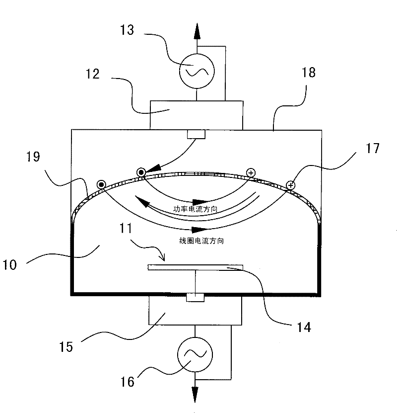
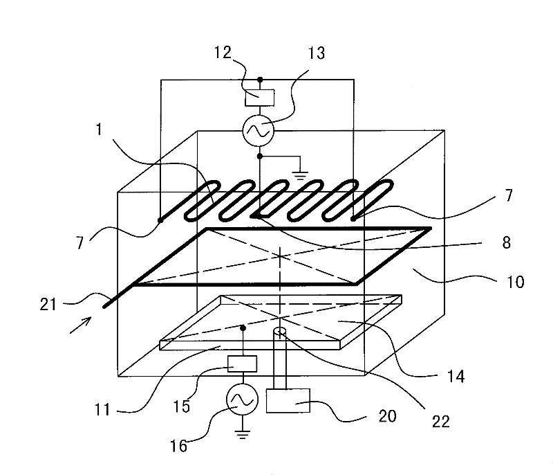
[0031] Such as figure 2 As shown, the device is mainly composed of a reaction chamber 10, a workbench 11, an inductive radio frequency generator, a substrate radio frequency generator, a gas supply system and an exhaust system. Among them, the inductive RF generator is composed of an inductive coupling coil, an inductive RF matcher 12 and an inductive RF power supply 13 , and the substrate RF generator is composed of a substrate electrode 14 , a substrate RF matcher 15 and a substrate bias power supply 16 .

[0032]Reaction chamber 10 forms a processing space by shell, and workbench 11, inductively coupled coil and substrate electrode 14 are all arranged in reaction chamber 10, and wherein, workbench 11 is positioned at the bottom of reaction chamber 10 processing spaces and is used for installing processed substrate , the inductive coupling coil is located above the workben...


PUM

PropertyMeasurementUnit
thicknessaaaaaaaaaa
thicknessaaaaaaaaaa
lengthaaaaaaaaaa

Abstract

The invention relates to the field of semiconductor manufacturing devices and particularly relates to an inductive coupling plasma device (ICP) and an inductive coupling coil used in the ICP device. The ICP device comprises a reaction chamber (10), a workbench (11), the inductive coupling coil, an inductance radio frequency matcher (12) and an inductance radio frequency power supply (13); the ICPdevice is characterized in that the inductive coupling coil is arranged in the reaction chamber (10) and positioned above the workbench (11); the inductive coupling coil is composed of the same two planar gridiron coils (1) which are connected in parallel and symmetrically arranged; wherein, each planar gridiron coil (1) uses a copper tube (2) to be folded into a gridiron structure according to aU-shaped wave path on a plane, a ceramic insulating inner sleeve (5) is arranged in the copper tube (2), the inner cavity of the ceramic insulating inner sleeve (5) is taken as a cooling water channel, and a ceramic insulating outer sleeve (6) is arranged outside the copper tube (2). The ICP device and the inductive coupling coil have good distribution uniformity of magnetic field, high efficiency and smaller damage to the surface of a substrate, thereby being applicable to large-area thin film deposition, etching, surface treatment and other semiconductor processing technologies.

Description

technical field [0001] The invention relates to the field of semiconductor manufacturing equipment, in particular to an inductively coupled plasma device (ICP) and a radio frequency inductively coupled coil used in the device. The inductively coupled plasma device is a high-density inductively coupled plasma device driven by a very high frequency power source, and can be applied to processes such as film deposition, etching, and surface treatment (such as cleaning) in semiconductor manufacturing. Background technique [0002] In the semiconductor manufacturing process, the plasma reaction device is an important processing equipment, which is widely used in thin film deposition, etching and surface treatment processes. The plasma reaction device is generally composed of a reaction chamber, a workbench, an inductive coupling element, a driving power supply, a gas supply system, and an exhaust system. The electromagnetic field that excites the plasma is provided to the reactio...

Claims


Application Information

Patent Timeline
Patent Type & Authority Patents(China)
IPC IPC(8): H01F5/00
Inventor 刘宏刘晓晗袁洁静
Owner SUZHOU UNIV OF SCI & TECH
Why Eureka
Try Eureka