

Groove gate type source-leakage composite field plate heterojunction field effect transistor and preparation method thereof
A heterojunction field effect and leaky field plate technology, applied in the field of microelectronics, can solve the problems of complex manufacturing process, cumbersome process debugging, and lower device yield, so as to improve transconductance, reduce electric field, and increase breakdown voltage. Effect
A heterojunction field effect and leaky field plate technology, applied in the field of microelectronics, can solve the problems of complex manufacturing process, cumbersome process debugging, and lower device yield, so as to improve transconductance, reduce electric field, and increase breakdown voltage. Effect
CN101414623BActive Publication Date: 2010-08-11XIAN CETC XIDIAN UNIV RADAR TECH COLLABORATIVE INNOVATION INST CO LTD
Image
Smart ImageViewing Examples


Examples
Embodiment 1
Embodiment 2
Embodiment 3
Login to View More PUM
 Abstract
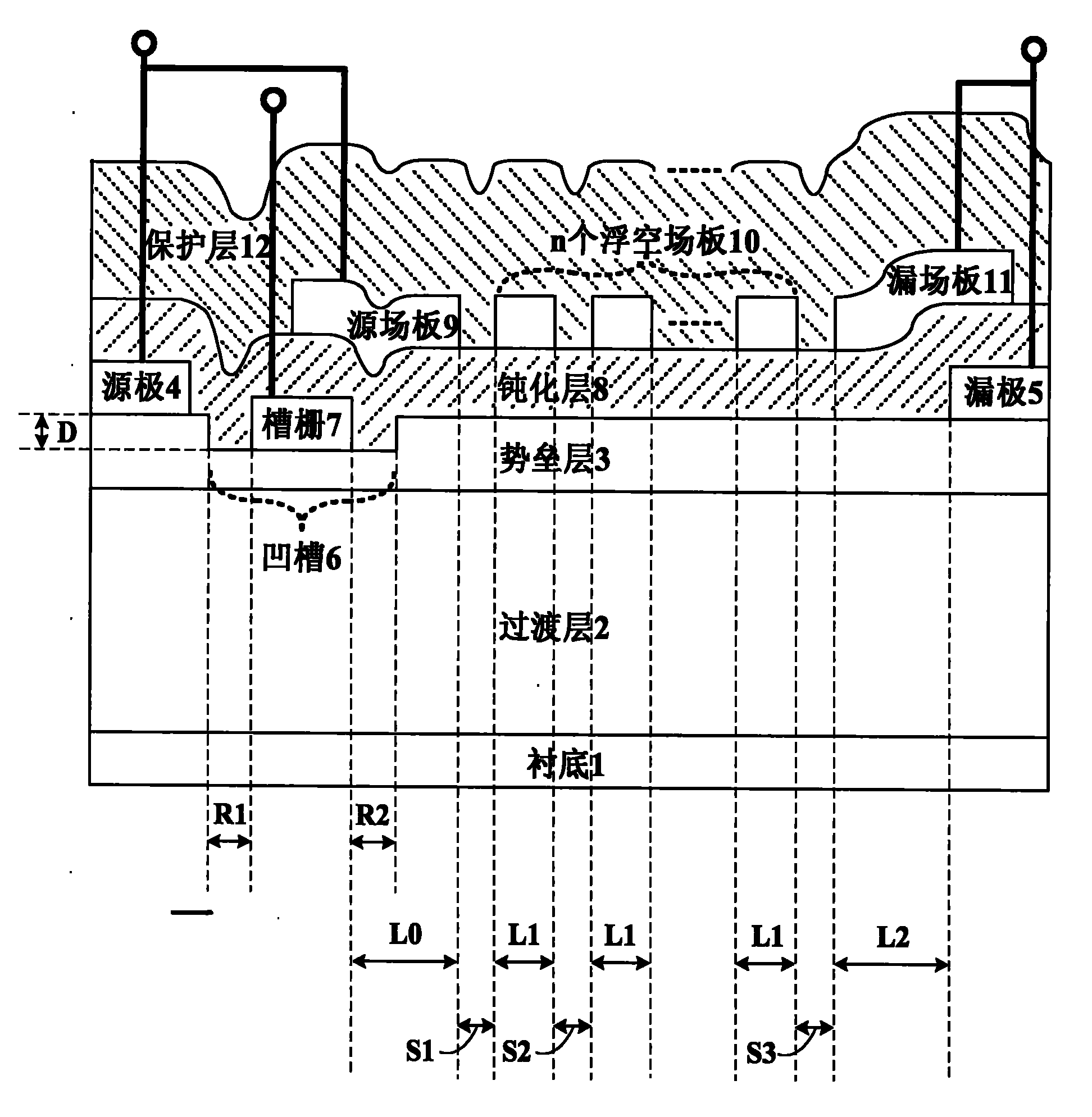
The invention discloses a groove-gate type source-drain composite field plate heterojunction field effect transistor and a fabrication method thereof. The transistor comprises, from bottom to top, a substrate (1), a transition layer (2), a barrier layer (3), a source electrode (4), a drain electrode (5), a groove gate (7), a passivation layer (8), a source field plate (9), a drain field plate (11) and a protection layer (12); the drain field plate is electrically connected with the drain electrode, the source field plate is electrically connected with the source electrode, wherein, a groove (6) is opened on the barrier layer (3); and n floating field plates (10) are deposited on the passivation layer arranged between the source field plate and drain field plate. All the floating field plate have the same size and are in a floating state, and the floating field plates are equidistantly distributed between the source field plate and the drain field plate. The n floating field plates, the source field plate and the drain field plate are completed on the passivation layer by one-time process. The transistor has the advantages of high yield, good reliability and high output power, and the transistor and the fabrication method can be used for fabricating power devices based on a wide band gap compound semiconductor material heterojunction.
Description
technical field The invention belongs to the field of microelectronics technology, and relates to semiconductor devices, in particular to a trench-gate source-drain composite field plate heterojunction field effect transistor based on a heterojunction structure of a wide bandgap compound semiconductor material, which can be used as a basic device of a high-power system . technical background In today's world, power semiconductor devices such as power rectifiers and power switches have been widely used in many power fields such as switching power supplies, automotive electronics, industrial control, radio communications, and motor control. Power semiconductor devices must have the following two important parameters, namely high breakdown voltage and low on-resistance. The Baliga figure of merit reflects the compromise relationship between breakdown voltage and on-resistance in power semiconductor devices. to explore. Silicon material is the most commonly used material for ...
Claims
Login to View More Application Information
Patent Timeline
11 Aug 2010
Publication
CN101414623B
- IPC
- H01L29/772; H01L29/06; H01L21/335
- Inventors
- 郝跃; 毛维