Wideband single layer microstrip patch antenna

A technology of microstrip patch antenna and microstrip patch, which is applied in the direction of antenna, electrical components, radiation element structure, etc., can solve the problem of narrow impedance bandwidth and achieve the effect of small cross section and simple structure

Active Publication Date: 2009-04-29
CHINA ELECTRONIC TECH GRP CORP NO 38 RES INST
View PDF0 Cites 34 Cited by
  • Summary
  • Abstract
  • Description
  • Claims
  • Application Information

AI Technical Summary

Problems solved by technology

[0009] In order to solve the shortcomings of the existing common microstrip antenna with narrow impedance bandwidth, the pres

Method used


Image

  • Wideband single layer microstrip patch antenna
  • Wideband single layer microstrip patch antenna
  • Wideband single layer microstrip patch antenna

Examples


Embodiment 1

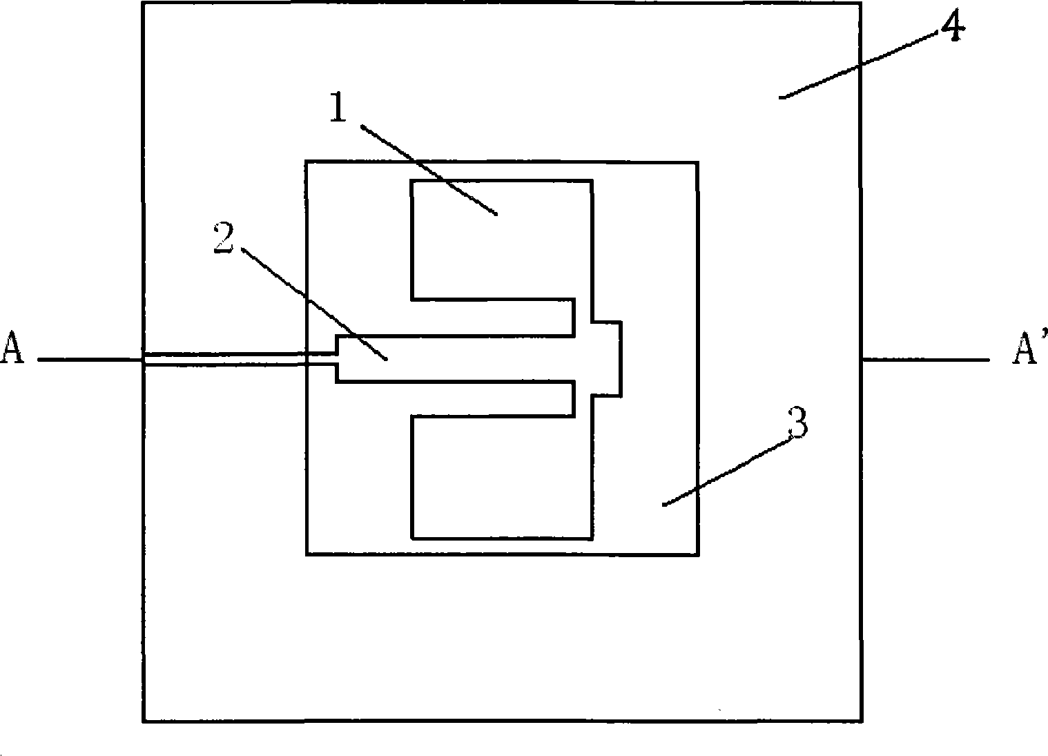
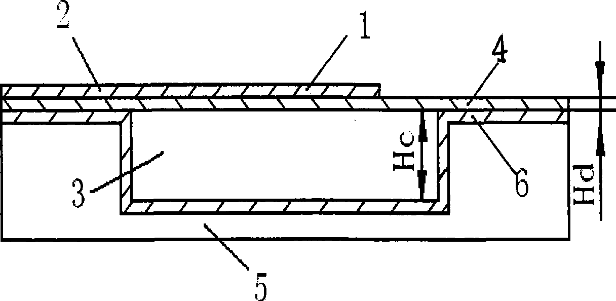
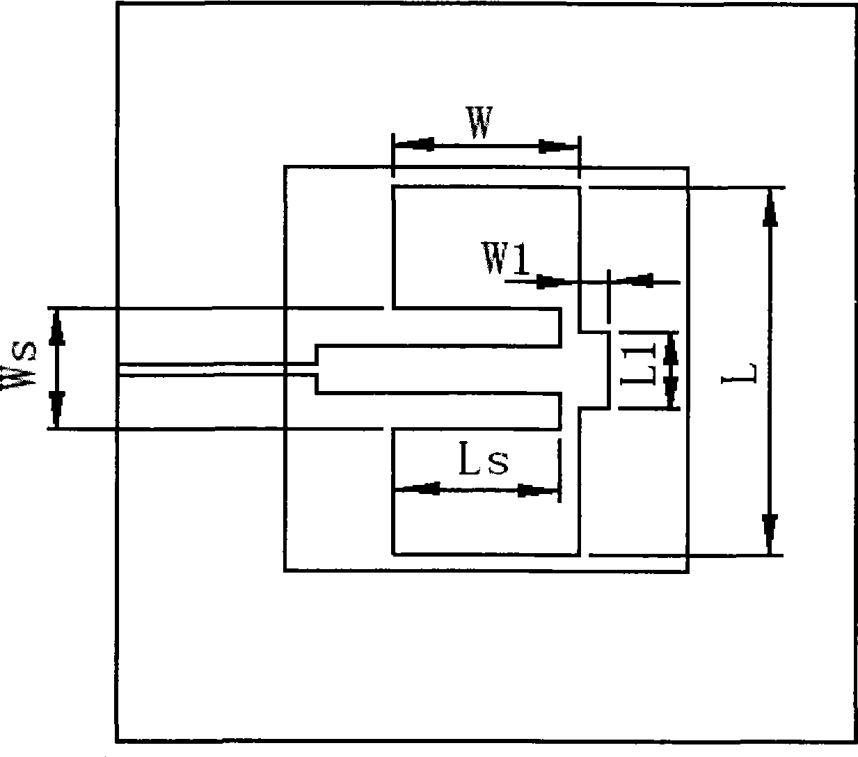
[0036] see figure 1 and figure 2 A broadband metal cavity-backed single-layer convex microstrip patch antenna includes a convex microstrip patch 1, a stepped coplanar microstrip line 2 with two widths, a back cavity 3, a microstrip dielectric plate 4, Structural support plate 5 and metal ground 6.

[0037] One end of the coplanar microstrip line 2 with two widths is inserted into the patch antenna through the slot on the convex microstrip patch, and the other end of the feeding microstrip line 2 is located at the edge of the microstrip dielectric plate 4;

[0038] The back of the microstrip dielectric plate 4 other than the corresponding part of the microstrip patch 1 is provided with a metal formation 6, and the back of the entire microstrip dielectric plate 4 is also provided with a structural support plate 5, and the structural support corresponding to the microstrip patch 1 The middle part of the plate 5 is a concave back cavity 3, and the inner surface of the concave b...

Embodiment 2

[0049] A preferred embodiment of the present invention is shown in Figure 7, which is an 8-element microstrip antenna line array applied to the X-band. This line array is formed by four 2-element arrays that are translated along a straight line, and the reverse phase feeding method is used between the 2 elements. , 8 convex microstrip patches 1 are connected with a coplanar 1:8 microstrip power dividing network 7 to form a line array, and finally are vertically welded with a coaxial connector 8 .

Embodiment 3

[0051] Another preferred embodiment of the present invention is shown in Fig. 8, and this 8 * 8 microstrip antenna sub-array is formed by the 8-element linear array shown in Fig. 7 and is translated along the same direction, and this sub-array is connected with T / R assembly, supplemented by The power supply, wave control and installation structural parts can be expanded into large sub-array active phased array antennas.


PUM

PropertyMeasurementUnit
Sizeaaaaaaaaaa
Sizeaaaaaaaaaa
Widthaaaaaaaaaa

Abstract

The invention relates to a wide band one-layer microstrip patch antenna, which solves the problem of narrow impedance width in the currently common microstrip antenna. The microstrip patch of the antenna is a one-layer microstrip patch; one end of a stair-stepping coplane microstrip line with two widths is inserted in the patch antenna by the open slot on a convex microstrip patch, and the other end of a feeding microstrip line is positioned at the edge of a microstrip dielectric-slab; a concave metal carinal cavity is arranged at the back surface of the microstrip dielectric-slab excluding the position corresponding to the microstrip patch and in the middle of structural mounting plate. The wide band one-layer microstrip patch antenna can form a large microstrip patch antenna array easily, which is in favor of impedance matching of the antenna, the subnetwork design for microstrip work, the weight reduction of the antenna and the bandwidth widening of the antenna; the wide band one-layer microstrip patch antenna of the invention has the advantages of simple and compact structure and small cross section, which improves the telecommunication performance and reduces the whole weightof the antenna array.

Description

technical field [0001] The invention relates to an improved structure of a single-layer dielectric microstrip patch antenna, in particular to a wide-band, metal back cavity structure, thin single-layer dielectric convex microstrip patch antenna. The invention can be used both for receiving and for transmitting radio waves. Background technique [0002] Broadband antennas are increasingly used in military and civilian applications. At the same time, in some specific applications, there are special requirements for the antenna array such as volume, weight, efficiency and environmental adaptability. For example: for aircraft / satellite platforms, antennas are required to have a thin profile, light weight, high efficiency and meet certain environmental application conditions. [0003] There are many types of radiating antennas suitable for planar antenna arrays, mainly waveguide slot antenna arrays, printed dipoles, and microstrip patch antenna arrays. The waveguide slot anten...

Claims


Application Information

Patent Timeline
IPC IPC(8): H01Q1/38H01Q13/08
Inventor 张智慧汪伟卢晓鹏张洪涛宋小弟
Owner CHINA ELECTRONIC TECH GRP CORP NO 38 RES INST
Why Eureka
Try Eureka