Forming method of shallow groove isolation and grinding method of semiconductor structure

A technology of isolation structure and grinding method, which is applied in semiconductor/solid-state device manufacturing, electrical components, circuits, etc., can solve problems affecting the reliability of components, and achieve the effect of improving uniformity and reducing height difference

Inactive Publication Date: 2009-05-06
UNITED MICROELECTRONICS CORP
View PDF0 Cites 11 Cited by
  • Summary
  • Abstract
  • Description
  • Claims
  • Application Information

AI Technical Summary

Problems solved by technology

This step-like drop will cause problems in subsequent processes, which in turn will affect the reliability of components

Method used


Image

  • Forming method of shallow groove isolation and grinding method of semiconductor structure
  • Forming method of shallow groove isolation and grinding method of semiconductor structure
  • Forming method of shallow groove isolation and grinding method of semiconductor structure

Examples


Embodiment Construction

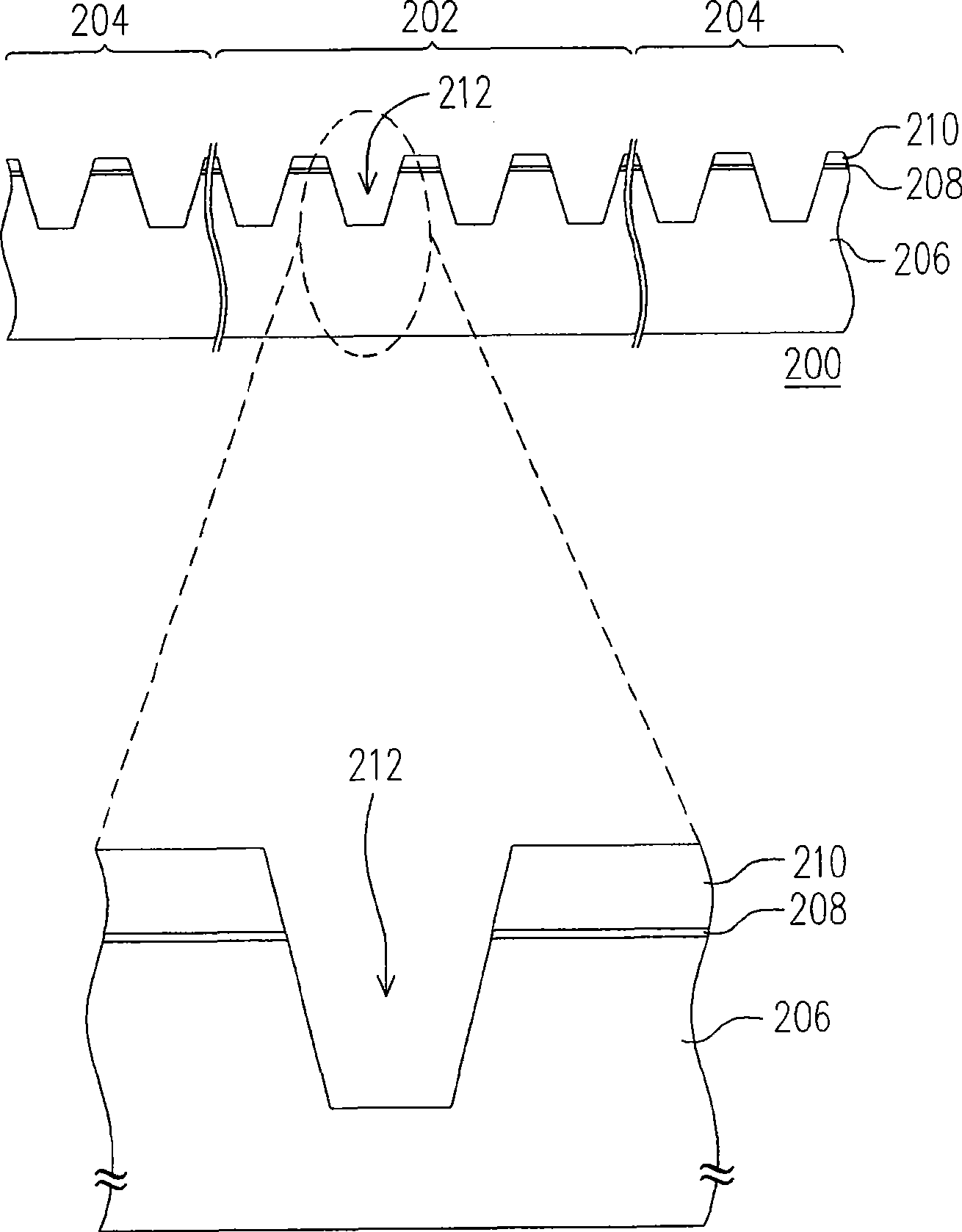
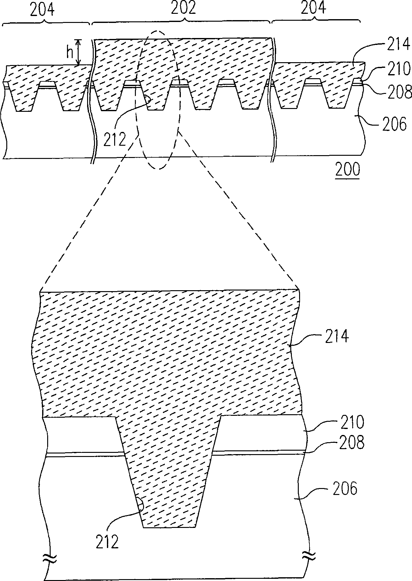
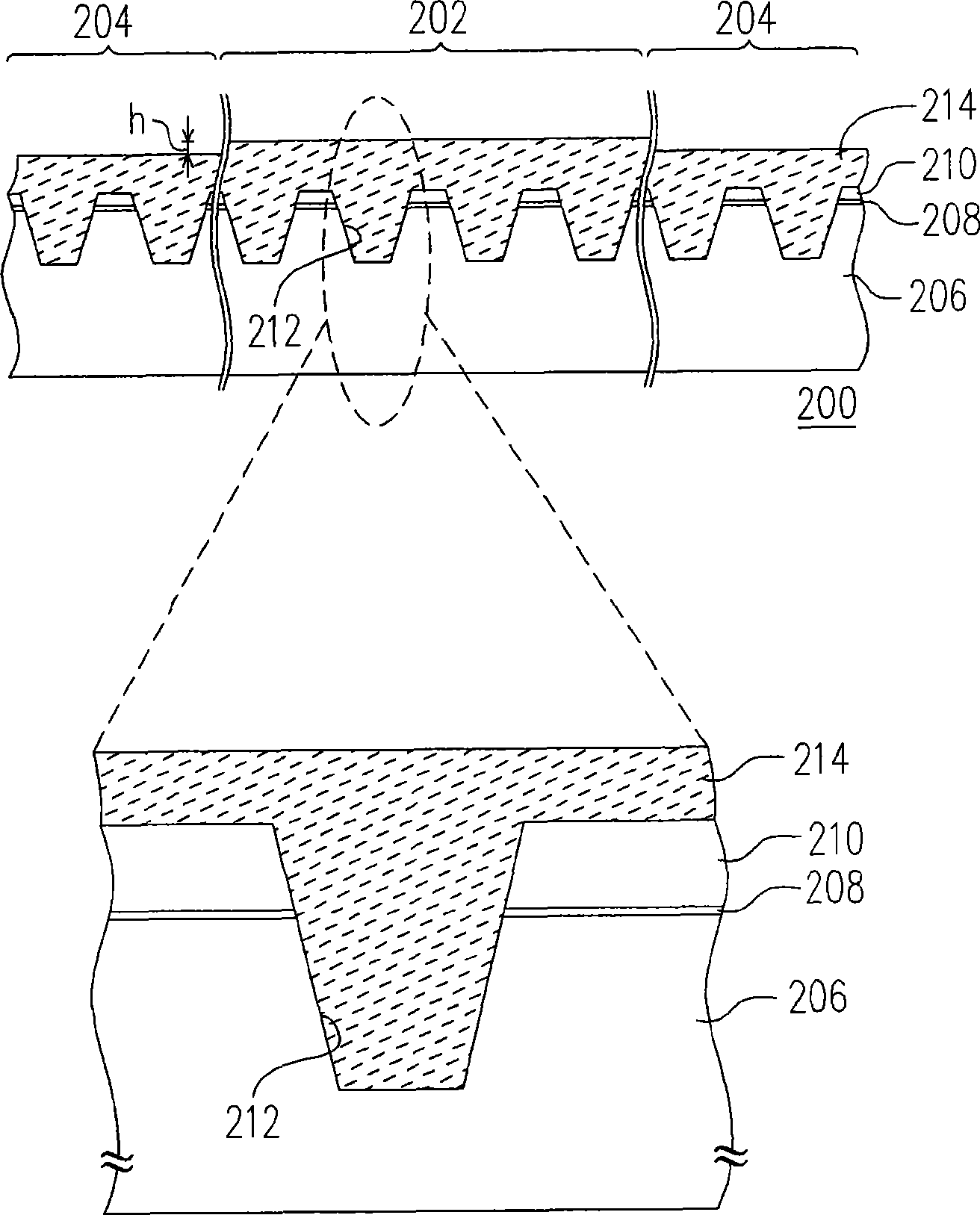
[0027] Figure 1A to Figure 1E It is a schematic cross-sectional view illustrating a formation process of a shallow trench isolation structure according to an embodiment of the present invention.

[0028] First, please refer to Figure 1A . A wafer 200 is provided that includes a semiconductor substrate 206 and can be divided into a central region 202 and an edge region 204 . Next, a pad layer 208 and a mask layer 210 are sequentially formed on the substrate 206 . The method for forming the pad layer 208 and the mask layer 210 is, for example, firstly forming a pad material layer, a mask material layer, and a patterned photoresist layer (not shown) on the substrate 206 in sequence. The material of the pad material layer is, for example, silicon oxide, and its formation method is, for example, thermal oxidation. The material of the mask material layer is, for example, silicon nitride, and its forming method is, for example, chemical vapor deposition. Then, using the pattern...


PUM


Abstract

The invention discloses a formation method of a shallow groove insulating structure and a grinding method of a semiconductor structure. The formation method of the shallow groove insulating structure comprises the following steps: forming a mask layer on the substrate of a wafer and removing the partial substrate which is not covered with the mask layer, so as to form a plurality of shallow grooves in the substrate; successively, forming a dielectric layer on the substrate and filling the dielectric layer into the shallow groove; then, carrying out first chemical-mechanical polishing process to remove the partial dielectric layer; and finally carrying out second chemical-mechanical polishing process to remove the partial dielectric layer and the mask layer, so that the surface of the dielectric layer is lower than that of the mask layer. The grinding velocity of the second chemical-mechanical polishing process is lower than that of the first chemical-mechanical polishing process; and the grinding selection ratio between the dielectric layer and the mask layer of the second chemical-mechanical polishing process is higher than that of the first chemical-mechanical polishing process. At last, the mask layer is removed.

Description

technical field [0001] The invention relates to a method for forming a semiconductor structure, and in particular to a method for forming a shallow trench isolation structure and a method for grinding the semiconductor structure. Background technique [0002] With the advancement of semiconductor technology, the size of components is also continuously reduced. When the size of the components enters the deep sub-micron range, or even finer dimensions, the probability of short circuits between adjacent components increases, so the isolation between components becomes very important. Generally speaking, an isolation layer is added between elements, and the more commonly used method today is a shallow trench isolation (STI) process. Since the shallow trench isolation structure is often an important key to component reliability, such as the occurrence probability of leakage current, the shallow trench isolation structure process plays an important role in advanced integrated cir...

Claims


Application Information

Patent Timeline
Patent Type & Authority Applications(China)
IPC IPC(8): H01L21/762H01L21/3105H01L21/02
Inventor 庄子仪
Owner UNITED MICROELECTRONICS CORP
Why Eureka
Try Eureka