

Preparation of tellurium nano-wire array based on physical vapour deposition
A technology of physical vapor deposition and tellurium nanowires, which is applied in ion implantation plating, metal material coating process, coating, etc.
- Summary
- Abstract
- Description
- Claims
- Application Information
AI Technical Summary
Problems solved by technology
Method used
Image

Examples
Embodiment 1
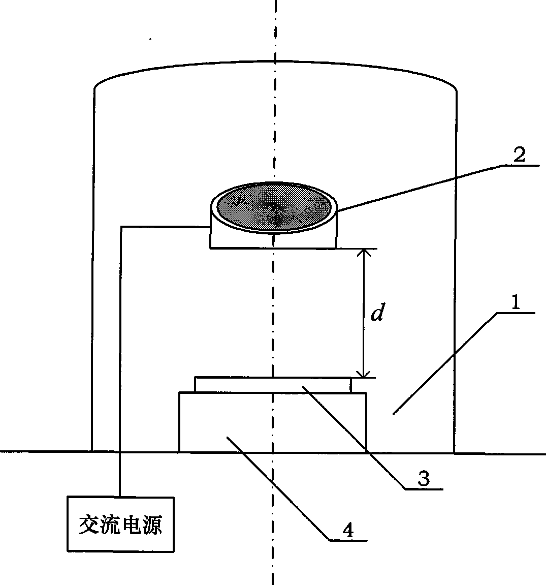
[0021] Put the tellurium Te elemental powder with a particle size of 5-10 μm into the tungsten boat 2 of the vacuum chamber 1 of the vacuum coating machine, place the glass substrate 3 on the sample stage 4, and adjust the distance d=10cm between the glass substrate 3 and the tungsten boat 2 ;
[0022] Seal the vacuum chamber 1, fill the vacuum chamber 1 with nitrogen for 3 minutes and stop (the nitrogen can be filled twice), then vacuumize the vacuum chamber 1 to make the vacuum degree in the vacuum chamber 1 reach 2.0×10 -4 Pa;
[0023] Set the deposition rate on the vacuum coating machine to 4nm / min, and the deposition time to 8h;
[0024] Turn on the AC power supply, adjust the output current to 165A; begin to deposit tellurium nanowire array films on the glass substrate 3 by physical vapor phase deposition.
[0025] After the preparation is completed, the AC power is turned off, and after natural cooling to room temperature, the glass substrate 3 with the tellurium nano...
Embodiment 2
[0029] Put the tellurium powder with a particle size of 5-20 μm into the tungsten boat 2 of the vacuum chamber 1 of the vacuum coating machine, place the glass substrate 3 on the sample stage 4, and adjust the distance d=6cm between the glass substrate 3 and the tungsten boat 2;
[0030] Seal the vacuum chamber 1, fill the vacuum chamber 1 with nitrogen for 5 minutes and then stop, then evacuate the vacuum chamber 1 to make the vacuum degree in the vacuum chamber 1 reach 3.0×10 -4 Pa;
[0031] Set the deposition rate on the vacuum coating machine to 8nm / min, and the deposition time to 5h;
[0032] Turn on the AC power supply, adjust the output current to 175A; begin to deposit and prepare the tellurium nanowire array thin film on the glass substrate 3 .
[0033] After the preparation is completed, the AC power is turned off, and after natural cooling to 28° C., the glass substrate 3 with the tellurium nanowire array thin film is taken out.
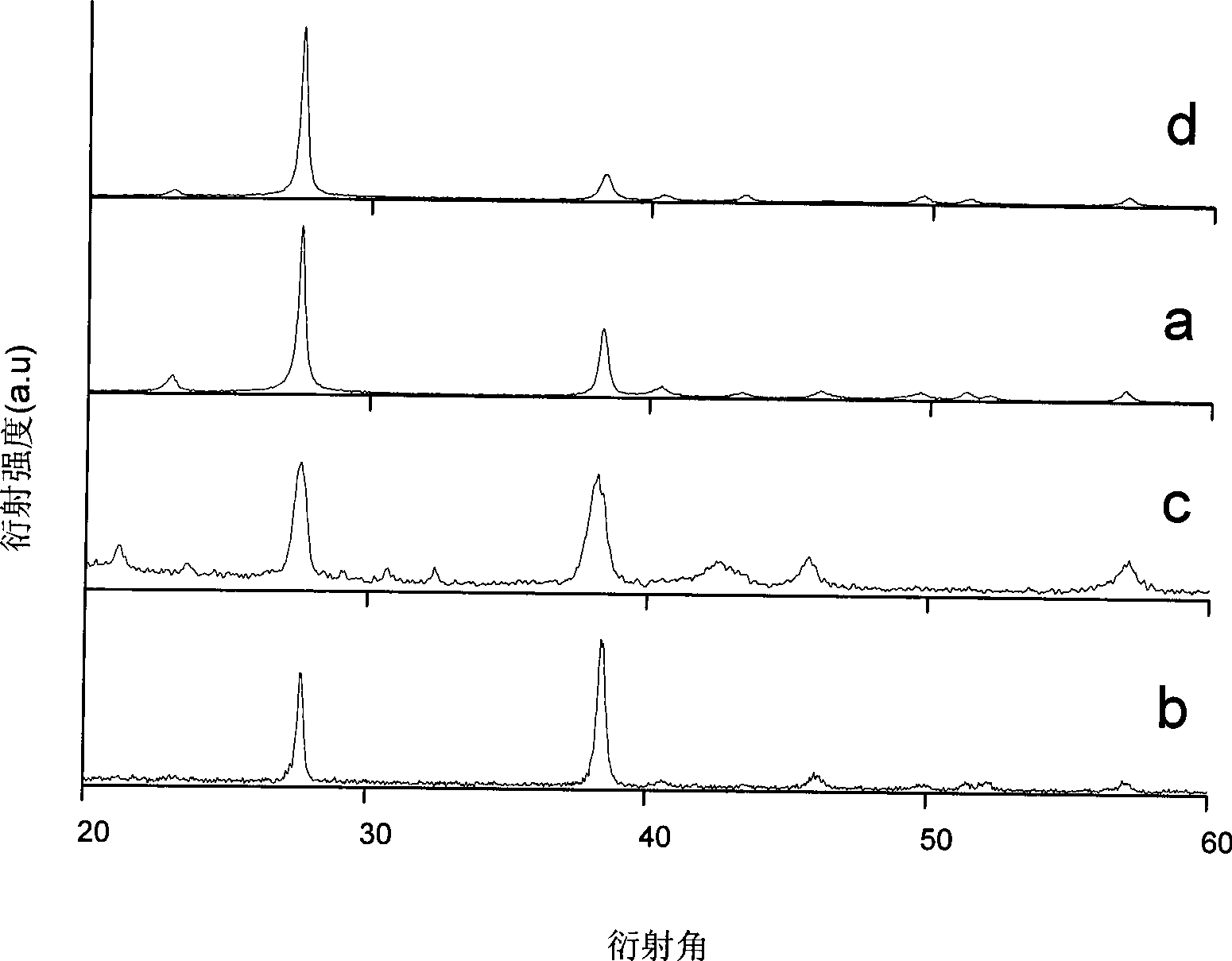
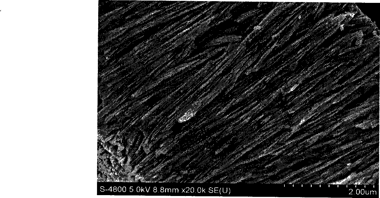
[0034] Adopt X-ray diffractometer...
Embodiment 3
[0037] Put the tellurium powder with a particle size of 10-20 μm into the tungsten boat 2 of the vacuum chamber 1 of the vacuum coating machine, place the glass substrate 3 on the sample stage 4, and adjust the distance d=9cm between the glass substrate 3 and the tungsten boat 2;
[0038] Seal the vacuum chamber 1, fill the vacuum chamber 1 with nitrogen for 3 minutes and then stop, then evacuate the vacuum chamber 1 to make the vacuum degree in the vacuum chamber 1 reach 5.0×10 -5 Pa;
[0039] Set the deposition rate on the vacuum coating machine to 12nm / min, and the deposition time to 6h;
[0040] Turn on the AC power supply, adjust the output current to 170A; begin to deposit and prepare the tellurium nanowire array thin film on the glass substrate 3 .
[0041] After the preparation is completed, the AC power is turned off, and after natural cooling to 22° C., the glass substrate 3 with the tellurium nanowire array thin film is taken out.
[0042] Adopt X-ray diffractomet...
PUM
| Property | Measurement | Unit |
|---|---|---|
| Diameter | aaaaa | aaaaa |
| Diameter | aaaaa | aaaaa |
| Diameter | aaaaa | aaaaa |
Abstract
Description
Claims
Application Information