Liquid crystal display panel and restoring method thereof

A liquid crystal display panel and repair method technology, applied in nonlinear optics, instruments, optics, etc., can solve problems such as easy breakdown, large graphics, poor display, etc., and achieve the effect of eliminating short circuits and improving yield

Inactive Publication Date: 2009-05-20
SHANGHAI SVA LIQUID CRYSTAL DISPLAY
View PDF0 Cites 20 Cited by
  • Summary
  • Abstract
  • Description
  • Claims
  • Application Information

AI Technical Summary

Problems solved by technology

Although the gold ball particles have a certain degree of elasticity, they still have a certain surface hardness due to the metal substance on the outer layer.
Therefore, under the action of an external force, the gold ball particles 7 with a diameter of several microns are likely to press through the insulating layer 12 on the thin signal lead 13, so that the signal lead layer 6 and the color filter on the array substrate side of two different signals The common electrode conductive layer 9 on the substrate side conducts and forms a short circuit, resulting in poor display
In addition, in the manufacturing process of liquid crystal displays, there are many occasions where static electricity occurs. The highest electrosta

Method used


Image

  • Liquid crystal display panel and restoring method thereof
  • Liquid crystal display panel and restoring method thereof
  • Liquid crystal display panel and restoring method thereof

Examples


Example Embodiment

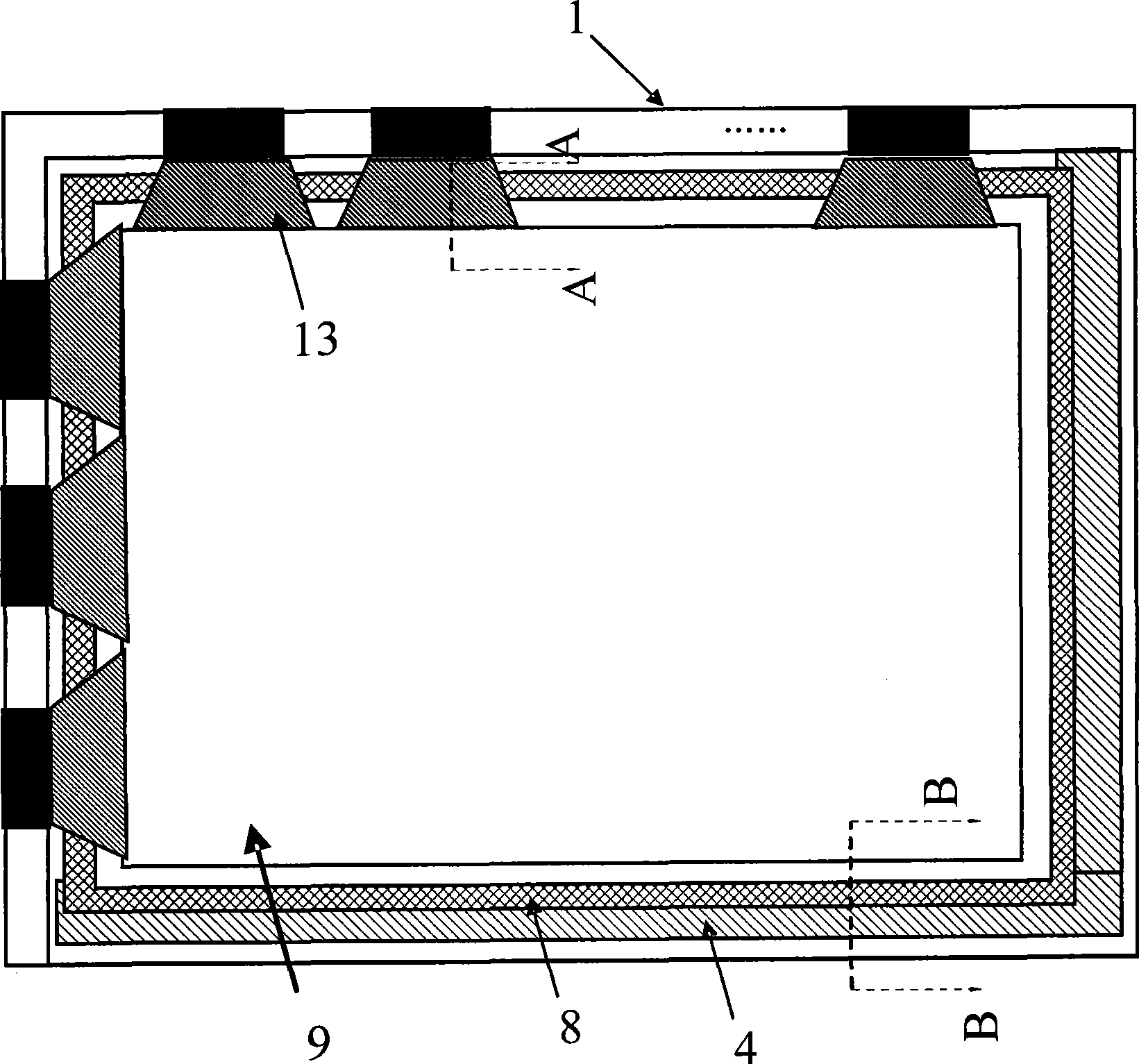
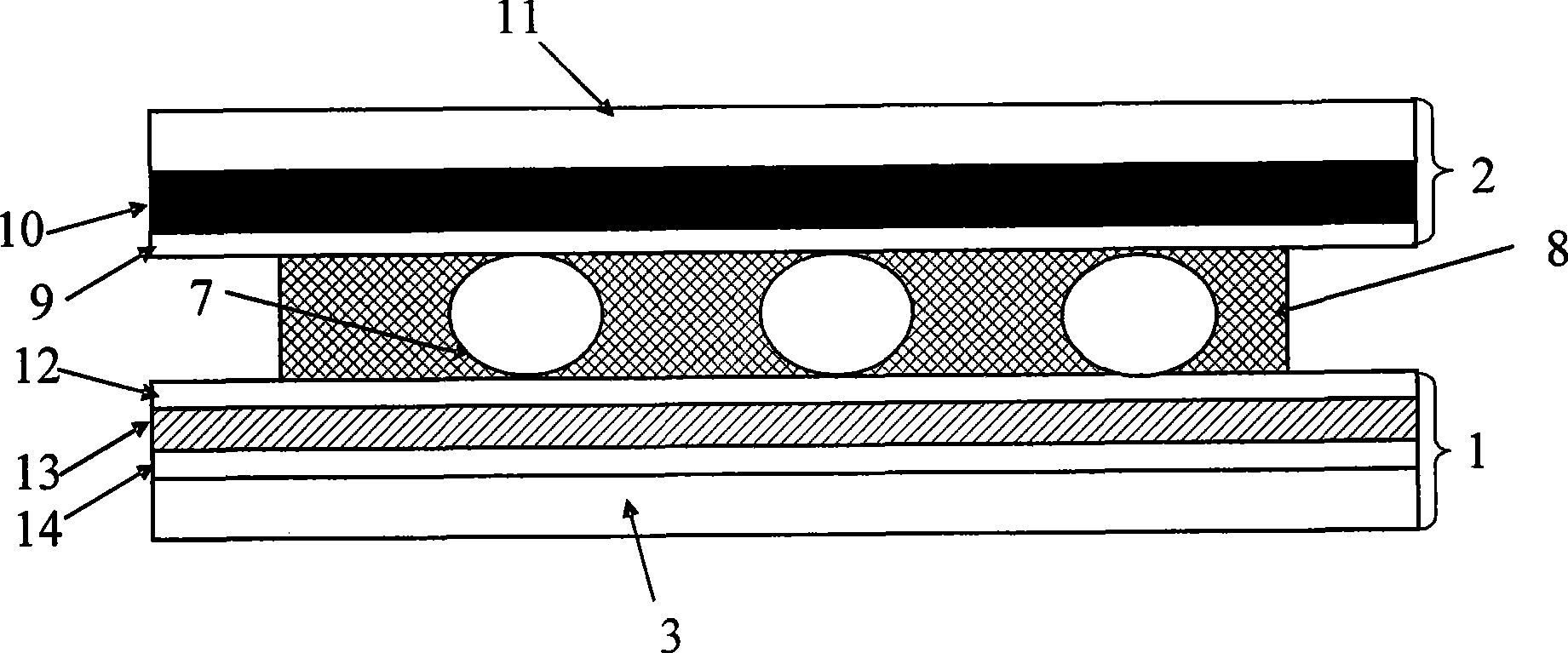
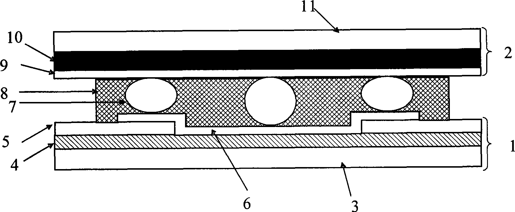
[0017] Hereinafter, the liquid crystal display panel and the repair method of the present invention will be described in further detail with reference to the accompanying drawings.

[0018] Figure 4 Is a schematic diagram of the structure of the first embodiment of the liquid crystal display panel of the present invention; Figure 5 for Figure 4 Sectional view along the C-C direction. Such as Figure 4 , Figure 5 As shown, the liquid crystal display panel of the present invention includes a plurality of signal terminals CO, signal leads 33 connected to the signal terminals CO transmit signals to the display area, and the indium-tin oxide (ITO) conductive layer on the side of the color film substrate 22 29 surrounds the signal lead 33 and has a frame sealant layer 28 near the signal terminal. The frame sealant layer 28 is arranged between the array substrate 21 and the color filter substrate 22 and is used to bond the array substrate 21 and the color filter substrate 22, The li...


PUM

PropertyMeasurementUnit
Thicknessaaaaaaaaaa

Abstract

The invention relates to a liquid crystal display panel and a restoring method thereof. The liquid crystal display panel comprises an array substrate, a colored film substrate and signal leads on the array substrate, wherein restoring wires overlapped with the signal leads are arranged among the signal leads. The restoring method comprises: cutting off two ends of a shorted signal lead out of an applying range of a hermetical rim substratum by a laser beam, so as to ensure that two ends of the cut point are not communicated electrically; and then, dotting the overlapped area of the signal leads and the corresponding restoring wires by the laser beam, so as to puncture an insulating layer between each signal lead and each corresponding restoring wire, and melt and combine the signal lead and the corresponding restoring wire together, thereby communicating the signal lead and the corresponding restoring wire electrically. The liquid crystal display panel eliminates adverse display caused by short circuit between the signal lead and a gold ball particle through cutting off the shorted signal lead and utilizing the mode of continuing transferring signals by the restoring wire, thereby improving the yield of the liquid crystal display panel.

Description

Technical field [0001] The invention relates to a liquid crystal display panel and a repair method thereof, in particular to repairable display defects caused by short circuit between gold ball particles and signal leads. Background technique [0002] Traditional CRT displays rely on cathode ray tubes to emit electrons to hit the phosphor powder on the screen to display images, but the principle of liquid crystal display is completely different. Generally, a liquid crystal display device (LCD) has (also called a color filter substrate) and a lower substrate (also called an array substrate), which are spaced apart from each other and face each other. A plurality of electrodes formed on the two substrates face each other. Sandwiched between the upper substrate and the lower substrate, voltage is applied to the liquid crystal through the electrodes on the substrate, and then the arrangement of the liquid crystal molecules is changed according to the applied voltage to display the im...

Claims


Application Information

Patent Timeline
IPC IPC(8): G02F1/13G02F1/1362
Inventor 焦峰
Owner SHANGHAI SVA LIQUID CRYSTAL DISPLAY
Why Eureka
Try Eureka