MTM anti-fuse structure on through hole and preparation process thereof

A preparation process and anti-fuse technology, which is applied in the field of microelectronics, can solve problems such as increasing the lateral size of the anti-fuse structure, short-circuit failure of the upper and lower electrodes of the anti-fuse, and affecting the integration of anti-fuse units, so as to reduce overlay risk, elimination of short-circuit phenomenon, effect of size reduction

Inactive Publication Date: 2017-04-26
58TH RES INST OF CETC
View PDF2 Cites 2 Cited by
  • Summary
  • Abstract
  • Description
  • Claims
  • Application Information

AI Technical Summary

Problems solved by technology

[0005] In the antifuse structure, due to the contact hole process of the barrier metal and the top metal on the antifuse, the photolithography process of the process is added to the antifuse structure process, and the photolithography process has a very high tolerance Engraving accuracy requirements, overlay deviations can easily cause short-circuit failure of the upper and lower electrodes of the anti-fuse; in addition, due to the existence of contact holes, the contact area between the top metal and the upper barrier layer of the MTM anti-fuse is reduced, which affects the conductivity of the anti-fuse; The sidewall oxide layer formed by the antifuse contact hole is a part of the MTM antifuse structure. The existence of this part increases the lateral size of the antifuse structure and affects the integration of the antifuse unit.
[0006] In addition, the lithography process control of the antifuse contact hole is the key point of the antifuse structure process, and the overlay accuracy of lithography determines the yield and reliability of the antifuse. The engraving accuracy is high and the process is complicated, resulting in an increase in process cost

Method used


Image

  • MTM anti-fuse structure on through hole and preparation process thereof
  • MTM anti-fuse structure on through hole and preparation process thereof
  • MTM anti-fuse structure on through hole and preparation process thereof

Examples


Embodiment Construction

[0045] The present invention will be further described below in conjunction with specific drawings and embodiments.

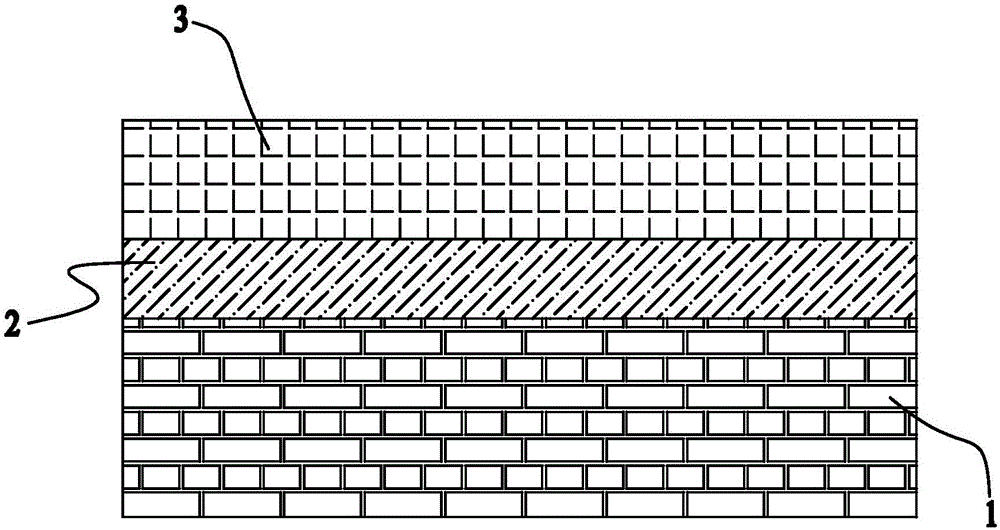
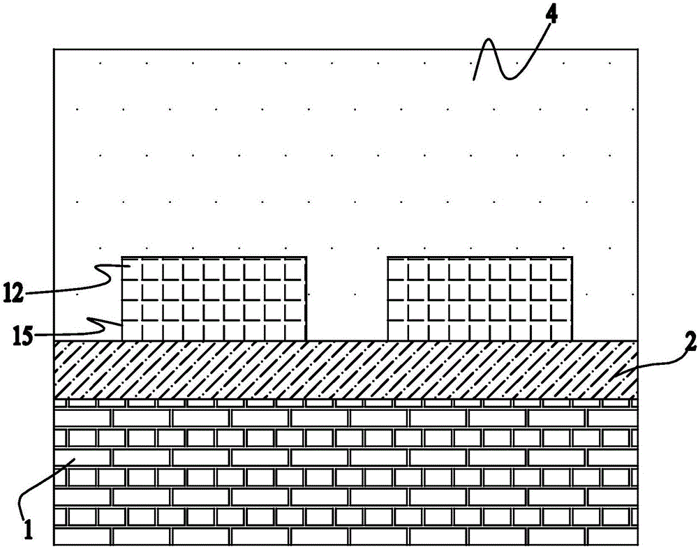
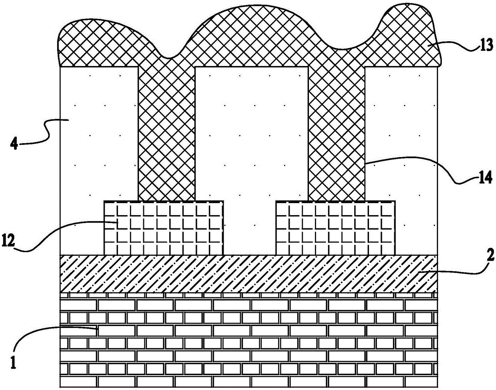
[0046] Such as Figure 12 As shown: In order to improve the integration level and improve the reliability of the antifuse, the present invention includes a substrate 1 and a device layer 2 located on the substrate 1; a fuse seal is pressed on the device layer 2 20. A lower fuse electrode is provided inside the fuse enclosure 20, and an upper fuse electrode 21 is provided outside the fuse enclosure 20, and the upper fuse electrode 21 is located directly above the lower fuse electrode ; An antifuse dielectric structure and an antifuse bottom barrier 17 are provided between the fuse upper electrode 21 and the fuse bottom electrode, and the antifuse bottom barrier 17 wraps the fuse bottom electrode in the fuse seal The top end of the anti-fuse medium structure is supported on the anti-fuse bottom barrier 17, and the upper fuse electrode 21 is supported on the anti...


PUM


Abstract

The invention relates to an MTM anti-fuse structure on a through hole and a preparation process thereof. The structure comprises a substrate and a device layer on the substrate. The device layer is pressed and covered by a fuse sealing body which is internally provided with a fuse lower electrode. A fuse upper electrode is arranged outside the fuse sealing body and is just above the fuse lower electrode. An anti-fuse dielectric structure and an anti-fuse bottom layer blocking body are arranged between the fuse upper electrode and the fuse lower electrode. The anti-fuse bottom layer blocking body coats the top end of the fuse lower electrode in the fuse sealing body. The anti-fuse dielectric structure is supported on the anti-fuse bottom layer blocking body, and the fuse upper electrode is supported on the anti-fuse dielectric structure. The structure of the MTM anti-fuse structure is compact, the times of lithography can be reduced, the process operation is simple, the process cost is reduced, the integration degree is raised, and the reliability of anti-fuse is improved.

Description

technical field [0001] The invention relates to an antifuse structure and a preparation process thereof, in particular to an MTM antifuse structure on a through hole and a preparation process thereof, belonging to the technical field of microelectronics. Background technique [0002] MTM antifuse is usually used in FPGA and PROM circuit products, and the antifuse unit in the circuit is programmed according to actual needs, so as to realize the logic function or storage function of the circuit. This type of circuit has the characteristics of strong confidentiality, good flexibility, and non-volatility, and has broad application prospects in aerospace and military fields. [0003] The MTM antifuse unit structure is located between two layers of metal wiring in the circuit. The antifuse unit is composed of an antifuse dielectric layer, two dielectric barrier layers and antifuse upper and lower electrodes. The antifuse unit is distributed from the top metal layer to the top laye...

Claims


Application Information

Patent Timeline
Patent Type & Authority Applications(China)
IPC IPC(8): H01L23/525H01L21/768
CPCH01L23/5252H01L21/76838
Inventor 王印权郑若成洪根深赵文彬徐海铭吴素贞
Owner 58TH RES INST OF CETC
Why Eureka
Try Eureka