Micro-complex type method for inducing electric field under the restrict of non-contact moulding board

A technology of electric field induction and micro-replication, which is applied in the direction of photolithography, optics, and optomechanical equipment on the pattern surface, which can solve the problems of unfavorable multi-layer overlay and replication, reduce processing costs and improve production efficiency , the effect of shortening the time

Inactive Publication Date: 2009-06-03
XI AN JIAOTONG UNIV
View PDF0 Cites 22 Cited by
  • Summary
  • Abstract
  • Description
  • Claims
  • Application Information

AI Technical Summary

Problems solved by technology

[0004] Aiming at the deficiencies such as the deformation of the template in the existing photolithography technology, which leads to replication defects, is not conducive to multi-layer overlay, and has certain film retention, the present invention uses a patterned template under the induction of an external electric field to Process high-precision, low-defect micro-nano structures on the corrosion-resistant adhesive layer

Method used


Image

  • Micro-complex type method for inducing electric field under the restrict of non-contact moulding board
  • Micro-complex type method for inducing electric field under the restrict of non-contact moulding board
  • Micro-complex type method for inducing electric field under the restrict of non-contact moulding board

Examples


Embodiment Construction

[0024] Below, the process of the electric field-induced micro-replication method under the constraint of a non-contact template will be described in detail in conjunction with the accompanying drawings:

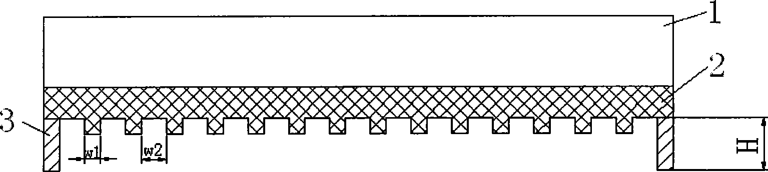
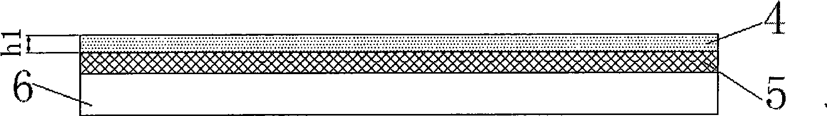
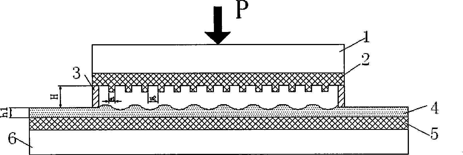
[0025] As shown, in SiO 2 The surface of the substrate 1 is vapor-deposited with a nano-indium tin metal oxide ITO glass layer 2, and the process of patterning and processing the supporting part 3 is carried out, as shown in the attached figure 1 shown in SiO 2 The surface conductive indium tin metal oxide ITO glass layer 5 on the surface of the substrate 6, and the process of spin-coating the corrosion resist adhesive layer 4 on the surface of the conductive indium tin metal oxide ITO glass layer 5, as attached figure 2 As shown, the process of pressing the prepared template on the corrosion resist adhesive layer 4 with a pressure of 20MPa, as shown in the attached image 3 shown in the template and SiO 2 The process of indirect DC power supply 7 between the substrates f...


PUM


Abstract

The invention belongs to the technical field of micro-nano manufacture, in particular to a micro-complex type method for inducing electric fields under the restrict of a non-contact moulding board, which comprises the following steps: 1) preparing a moulding board: depositing conductive nanometer indium-tin metal oxide ITO glass on a SiO2 base material to prepare a graphical moulding board; 2) vapor-depositing conductive nanometer indium-tin metal oxide ITO glass on the surface of the SiO2 base material; 3) pasting corrosion-proof glue on the surface of the SiO2 base material; 4) processing the prepared moulding board on the corrosion-proof glue layer; 5) circumscribing a DC source to allow the corrosion-proof glue to generate rheological deformation; 6) carrying out electric field to induce micro-complex type; and 7) exposing to ultraviolet to solidify the corrosion-proof glue so as to obtain a required micro-nano structure. The method has the advantages that the processing cost is low; the required time is short; and the production efficiency is improved, therefore, the method can be used for processing various MEMS / NEMS (micron electromechanical system / nanometer electromechanical system) devices such as a micro-fluidic device, a micro-sensor, a micro- brake, a raster, a minitype biochip, a photoelectron device, a solar battery and the like.

Description

technical field [0001] The invention belongs to the technical field of micro-nano manufacturing, and in particular relates to a micro-replica method for manufacturing micro-scale or nano-scale structures by using a template to constrain the electric field distribution under the induction of an electric field. Background technique [0002] The traditional optical projection lithography process uses X-rays, ultraviolet rays, etc., through a mask with a certain pattern structure for controllable exposure, and transfers the pattern on the mask to the resist that is pre-coated on the substrate and dried. Floor. Finally, a patterned resist layer is obtained by chemical development. Traditional optical projection lithography technology has been occupying a dominant position in the field of micro-nano manufacturing because it has been maturely developed in the field of semiconductor manufacturing. However, due to the continuous development of micro-nano manufacturing technology to...

Claims


Application Information

Patent Timeline
Patent Type & Authority Applications(China)
IPC IPC(8): G03F7/00
Inventor 刘红忠丁玉成李欣蒋维涛
Owner XI AN JIAOTONG UNIV
Why Eureka
Try Eureka