

Electronic component, semiconductor package and electronic device
A technology for electronic components and semiconductors, applied in the fields of semiconductor devices, semiconductor/solid-state device manufacturing, electric solid-state devices, etc., can solve problems such as reduced reliability, reduced adhesion, and reduced work efficiency
- Summary
- Abstract
- Description
- Claims
- Application Information
AI Technical Summary
Problems solved by technology
Method used
Image

Examples
no. 1 approach
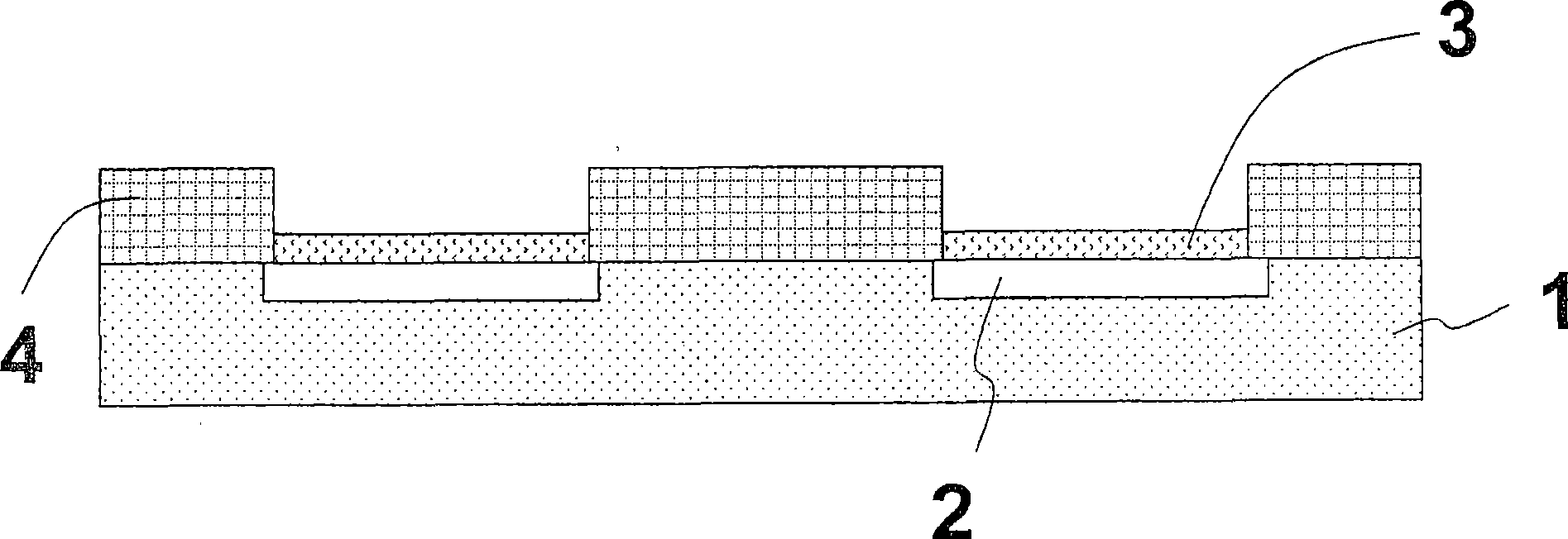
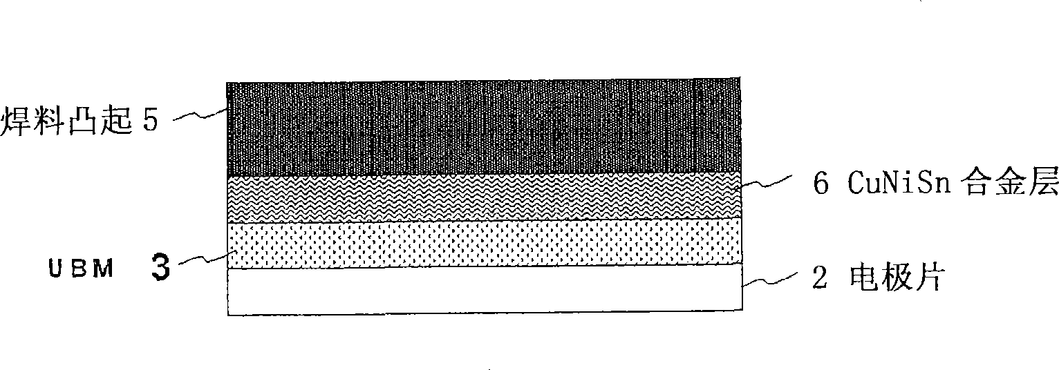
[0137] as in figure 1 As shown in , in one example of the electronic component 1 according to the present invention, a UBM (barrier metal layer) 3 is formed on an electrode pad 2 made of, for example, Al, Cu, and Ag formed on a substrate or a semiconductor element. The electrode pads are electrically connected to wirings in the substrate or semiconductor element.
[0138] UBM3 has any one of the following alloy layers formed at least on the side opposite to the side in contact with the electrode sheet: (1) a CuNi alloy layer containing 15 to 60 atomic % of Cu and 40 to 85 atomic % of Ni, ( 2) A CuNiP alloy layer containing Cu equal to or higher than 15 atomic %, Ni equal to or higher than 40 atomic %, and P higher than 0 atomic % and equal to or lower than 25 atomic %, or (3) containing 44 A CuNiP alloy layer having up to 60 atomic % of Cu, 29 to 40 atomic % of Ni, and 8 to 16 atomic % of P, while the Ni content (on an atomic basis) is at least 2.5 times the P content (on an...
no. 2 approach
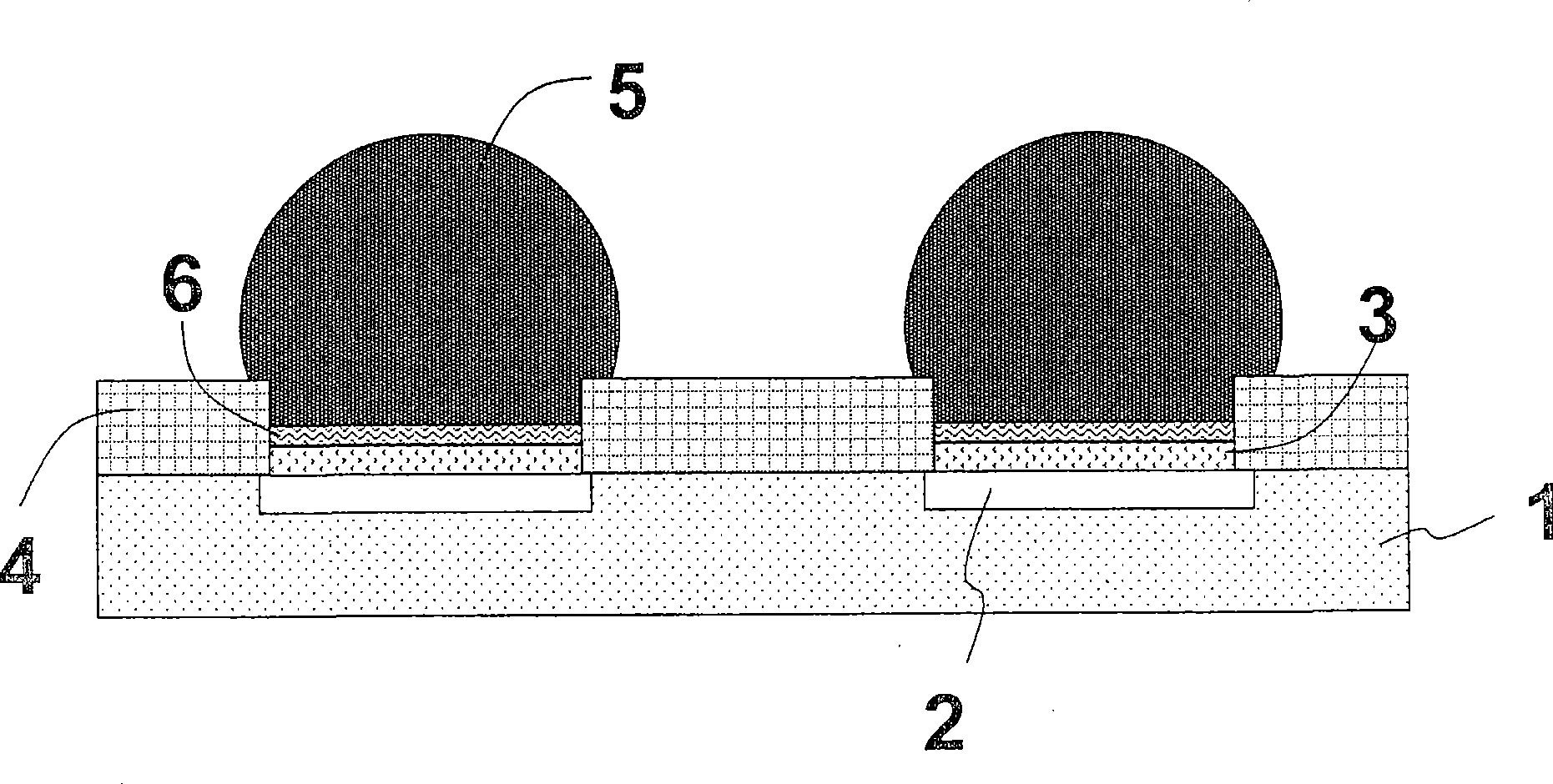
[0209] In addition to the above structure, the electronic component of the present invention can also have a structure containing more than two layers: such as Figure 10 As shown in , an electrode sheet 2 made of Al, Cu, Ag or other elements, and a CuNi alloy layer or a CuNiP alloy layer 3 , with an intermediate layer 9 between the electrode sheet 2 and the alloy layer 3 . In this case, the composition of the top barrier metal layer attached to the CuNiSn alloy layer must be CuNi alloy or CuNiP alloy.
[0210] Examples of the material of the intermediate layer 9 may include Ni, Cu, Pd, Pt, Fe, Co, Cr, and Ti, and NiP alloys, NiB alloys, and CoP alloys containing any of the above metals. The above alloy in the intermediate layer has the following composition:
[0211] -NiP alloy: NiP alloy containing 2 to 25 atomic % of P
[0212] -NiB alloy: NiB alloy containing 1 to 10 atomic % of B
[0213] -CoP alloys: CoP alloys containing 2 to 25 atomic % of P
[0214] One reason for...
no. 3 approach
[0218] Electronic parts that have been described in the present invention refer to general components forming circuits, such as those formed on printed substrates, flexible substrates, ceramic substrates, glass-ceramic substrates, and semiconductor substrates, as well as chip capacitors and chip resistors.
[0219] The semiconductor package of the present invention has electronic components electrically connected by UBM, solder bumps, and the like. Examples of electronic components may include substrates such as motherboard substrates, interposer substrates, semiconductor packages, printed substrates, flexible substrates, ceramic substrates, glass-ceramic substrates, and semiconductor substrates, and semiconductor chips (semiconductor elements). Examples of connections between these electronic components may include substrate-to-substrate connections, semiconductor element-to-semiconductor element connections, and substrate-to-semiconductor element connections.
[0220] Figu...
PUM
| Property | Measurement | Unit |
|---|---|---|
| thickness | aaaaa | aaaaa |
| thickness | aaaaa | aaaaa |
| thickness | aaaaa | aaaaa |
Abstract
Description
Claims
Application Information