Micro-nano fabrication method for auxiliary etch by combining focused ion beam injection and xenon fluoride gas

A focused ion beam, gas-assisted technology, applied in the process of producing decorative surface effects, microstructure technology, gaseous chemical plating, etc., can solve problems affecting processing accuracy, improve processing quality, reduce impact, The effect of improving the efficiency of structure preparation

Inactive Publication Date: 2009-06-17
TIANJIN UNIV
View PDF0 Cites 12 Cited by
  • Summary
  • Abstract
  • Description
  • Claims
  • Application Information

AI Technical Summary

Problems solved by technology

However, for focused ion beam milling technology, the redepos

Method used


Image

  • Micro-nano fabrication method for auxiliary etch by combining focused ion beam injection and xenon fluoride gas
  • Micro-nano fabrication method for auxiliary etch by combining focused ion beam injection and xenon fluoride gas
  • Micro-nano fabrication method for auxiliary etch by combining focused ion beam injection and xenon fluoride gas

Examples


Embodiment 1

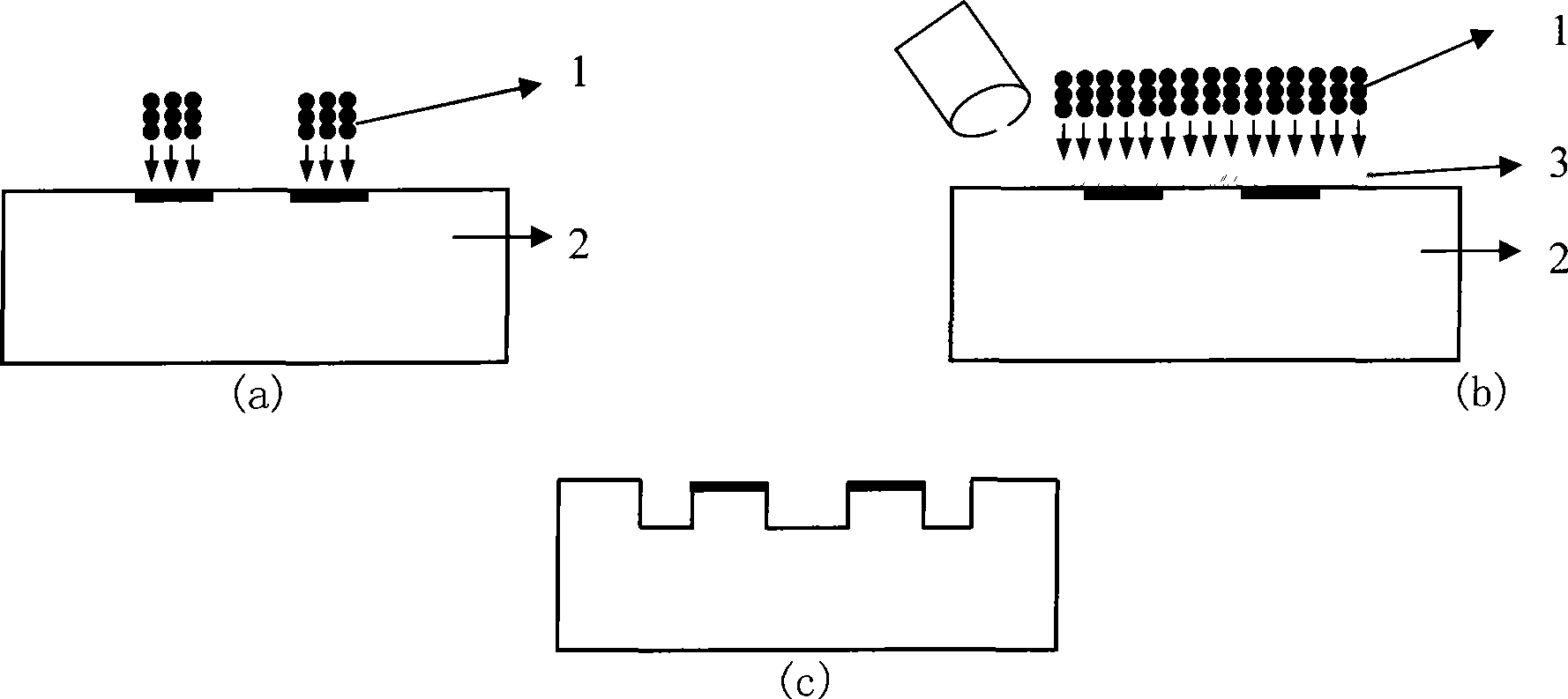
[0026] Using 30kV accelerating voltage and 30pA gallium ion beam, with 1.4×10 21 ion / m 2 Ion dose Ion implantation was performed on the monocrystalline silicon sample, the implantation time was 210 seconds, and the ion implantation method was uniform implantation. Subsequently, XeF was performed with a beam current of 30kV and 30pA 2 The gas-assisted etching is performed for 8 seconds, and the processing range of the assisted etching is 18 microns×12.5 microns. After the auxiliary etching is stopped, a microelectrode structure with a height of about 100 nanometers protruding from the ion implantation area will be generated, such as figure 2 shown.

Embodiment 2

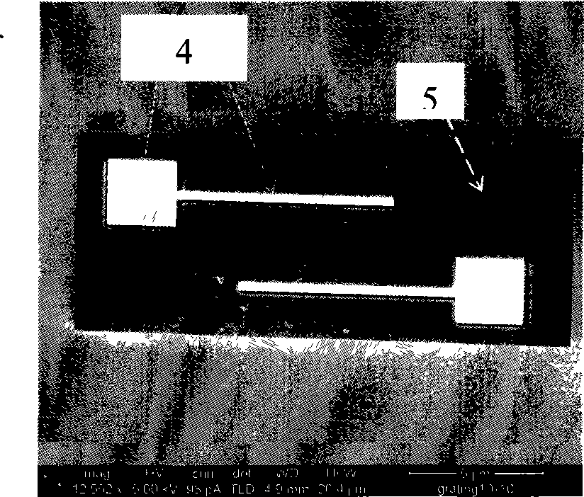
[0028] The single crystal silicon sample was implanted with 30kV accelerating voltage and 30pA gallium ion beam. The ion implantation method was implanted according to the law of the grating structure. The ion implantation processing range was 5 microns*5 microns, and the ion implantation time was 40 seconds. Subsequently, XeF was performed with a beam current of 30kV and 30pA 2 The gas-assisted etching is performed for 2 seconds, and the processing range of the assisted etching is 5.5 microns×5.8 microns. After the auxiliary etching is stopped, a micro-grating structure with a depth of about 100 nanometers will be generated with the ion implantation region as a protrusion, such as image 3 shown.

Embodiment 3

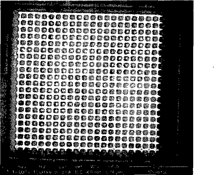
[0030] The single crystal silicon sample was implanted with 30kV accelerating voltage and 50pA gallium ion beam. The ion implantation was carried out according to the sinusoidal distribution law. The implantation time of a single micro-sine structure was 60 seconds, and the micro-sine diameter was 5 microns. sinusoidal structure. Subsequently, XeF was performed using 10kV and 23pA beam current 2 The gas-assisted etching is performed for 15 seconds, and the processing range of the assisted etching is 21 microns×21 microns. After the auxiliary etching is stopped, a micro-sinusoidal structure with a peak-to-valley value of about 100 nanometers protruding from the ion implantation region will be generated, such as Figure 4 shown.


PUM


Abstract

The invention relates to a micro-nano processing method based on injection of focused ion beams and etching of auxiliary gas, which comprises the following steps: placing a substrate to be processed in a focused ion beam sample chamber; observing appearance of the substrate through an ion beam imaging system; carrying out ion injection and processing on the substrate by using the focused ion beams according to a target processing pattern; and carrying out micro-nano processing on an ion injected area by in situ using a method of auxiliary etching of focused ion beam xenon fluoride gas in the focused ion beam sample chamber. The method is stable and reliable, not only can remarkably improve preparation efficiency, but also improves processing flexibility, can effectively reduce influence of processing re-deposition, and remarkably improves processing accuracy and processing quality.

Description

technical field [0001] The present invention relates to a micro-nano processing method, more specifically, to a micro-nano processing method based on focused ion beam implantation and assisted gas etching, which can be used in MEMS, micro-nano manufacturing, biochemical analysis, optics and communication and other fields. Background technique [0002] Focused ion beam (FIB) processing technology has been widely used in the processing of micro-nano structures. Focused ion beam systems are capable of not only removing material (milling) but also adding material (ion implantation and deposition). Ion implantation is the use of high-energy ions to bombard the surface of the sample, so that the high-energy ions are injected into the sample. The incident ions gradually lose energy by colliding with the atoms in the workpiece, and finally stay on the surface of the sample. [0003] Compared with the traditional mask implantation method, using the focused ion beam system for fixed...

Claims


Application Information

Patent Timeline
IPC IPC(8): B81C1/00
Inventor 房丰洲徐宗伟胡小唐
Owner TIANJIN UNIV
Why Eureka
Try Eureka