Film bulk acoustic wave resonator and preparation method thereof

A thin-film bulk acoustic wave and resonator technology, which is applied in the direction of electrical components and impedance networks, can solve the problems of increasing processing equipment and silicon wafer thickness precision control, unfavorable CMOS chip processing, and increased FBAR insertion loss, etc., to achieve Reduce equipment requirements, increase process difficulty, and reduce insertion loss

Inactive Publication Date: 2009-06-24
UNIV OF ELECTRONICS SCI & TECH OF CHINA
View PDF2 Cites 96 Cited by
  • Summary
  • Abstract
  • Description
  • Claims
  • Application Information

AI Technical Summary

Problems solved by technology

However, these improved structures still have disadvantages: 1. In order to ensure that the FBAR has good frequency stability, the area between the bottom electrode and the top electrode needs to be very flat
It is necessary to use high-precision CMP technology to smooth the silicon surface, which increases the requirements for processing equipment and thickness precision control of silicon wafers, and is not conducive to processing FBAR on CMOS chips
2. Usually there is an amorphous transition region with a certain thickness on the piezoelectric layer. When the application frequency of FBAR rises from a few GHz to tens of GHz, the piezoelectric layer will be made thinner and thinner, and the piezoelectric film with preferred orientation The ratio of the layer thickness to the thickness of the amorphous transition region will be reduced, which will lead to a larger insertion loss and a lower Q value of the FBAR
This limits the development of FBAR in the direction of high frequency

Method used


Image

  • Film bulk acoustic wave resonator and preparation method thereof
  • Film bulk acoustic wave resonator and preparation method thereof
  • Film bulk acoustic wave resonator and preparation method thereof

Examples


specific Embodiment approach

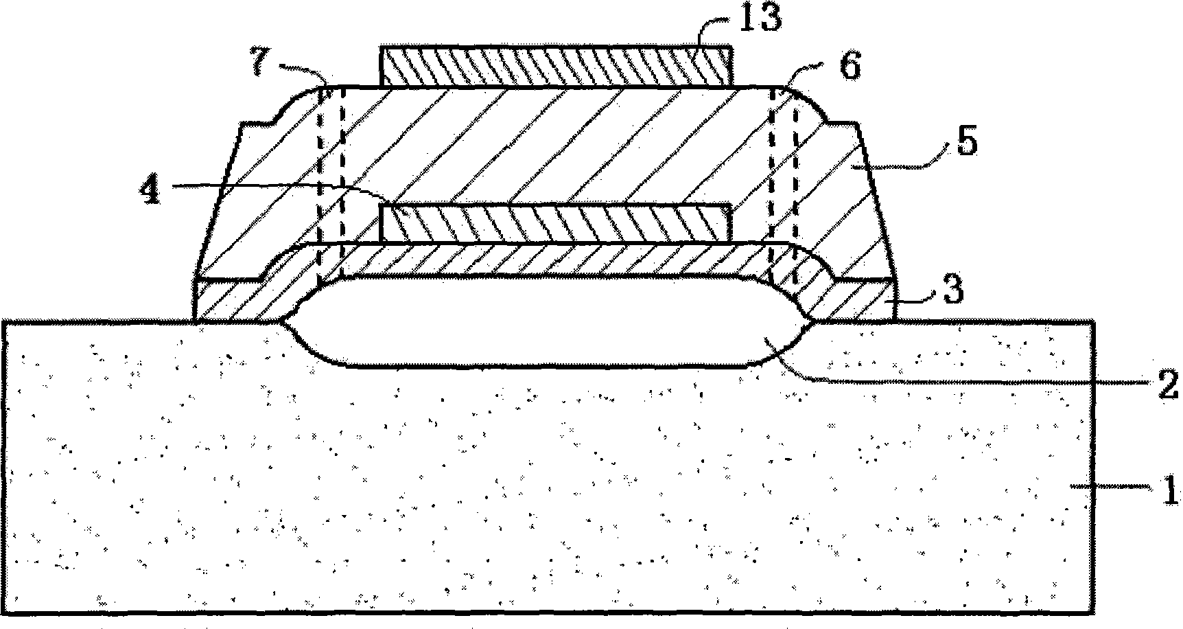
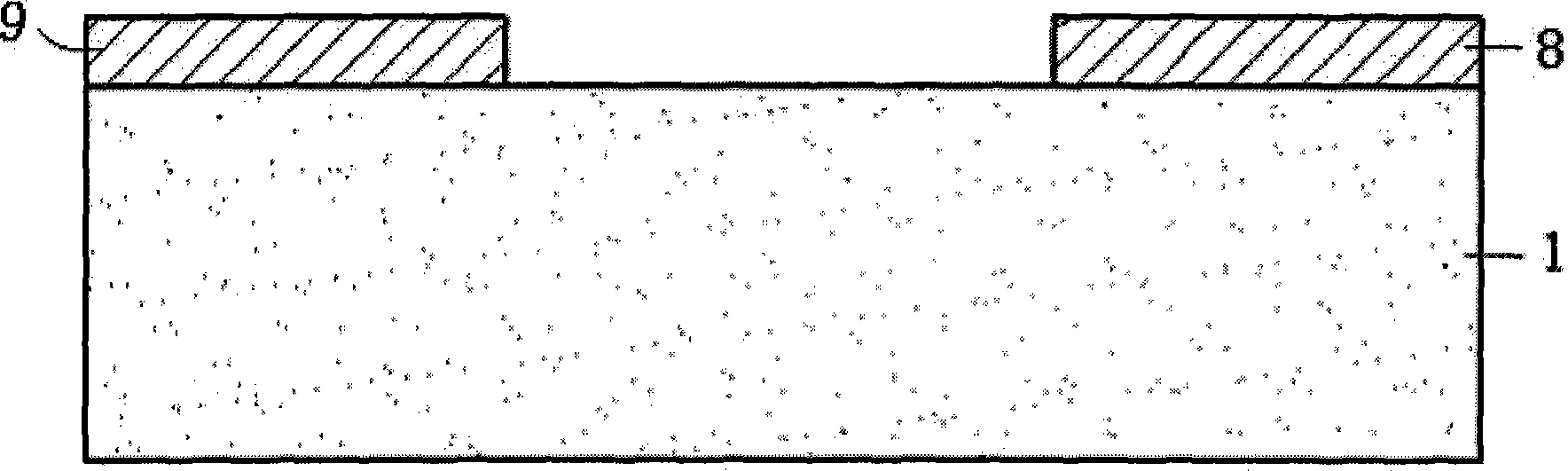
[0051] 1) Deposit a layer of silicon nitride with a thickness of about 100 nm on the surface of the polished silicon 1 by CVD. The polished surface may be (100), (110) or (111) oriented. Then use photolithography to remove the silicon nitride corresponding to the area of ​​the sacrificial layer, leaving the silicon nitride at the part of 8 and 9 as image 3 shown.

[0052] 2) On the silicon surface on which the silicon nitride 8 and 9 have been grown, a layer of silicon dioxide 10 is grown in the area where the silicon nitride is removed by wet thermal oxidation treatment. The silicon dioxide has a thickness between 400nm and 800nm. Such as Figure 4 shown.

[0053] 3) After the above steps, remove the residual silicon nitride 8, 9 on the silicon surface, leaving the silicon dioxide 10 part. Such as Figure 5 shown.

[0054] 4) After the above steps, an amorphous aluminum nitride layer 11 of about 100 nm is grown on the silicon surface, and then a layer of metal is grow...


PUM


Abstract

The invention discloses a thin film bulk acoustic wave resonator which comprises a substrate, a buffer layer, a piezoelectric layer and electrodes, and is characterized in that 1. A smooth concave groove and the buffer layer are arranged on the upper end surface of the substrate; the buffer layer crosses the concave groove and forms an air gap provided with a smooth upper convex edge with the substrate, and completely covers the air gap; the height of the lower top surface of the air gap is less than that of the substrate, and the air gap has flat surface and even change edge; 2. The edge of the buffer layer, which is contacted with the air gap and is close to the substrate is in smooth and outer-convex shape; the piezoelectric layer is arranged on the buffer layer; the electrodes include a bottom electrode and a top electrode; the bottom electrode is arranged in the piezoelectric layer on the buffer layer; the top electrode is arranged on the piezoelectric layer. The thin film bulk acoustic wave resonator has ingenious structure; a FBAR with stable structure and low loss can be fabricated on the substrate through the method, and the CMP process is avoided, so the thin film bulk acoustic wave resonator can be integrated into a CMOS chip conveniently.

Description

technical field [0001] The invention relates to the technical field of thin-film bulk acoustic wave resonators, in particular to a thin-film bulk acoustic wave resonator and a preparation method thereof. Background technique [0002] The multi-functional development of wireless communication terminals has put forward high technical requirements for radio frequency devices such as miniaturization, high frequency, high performance, low power consumption, and low cost. Traditional surface acoustic wave devices have large insertion loss in the high-frequency band above 2.4GHz, and microwave dielectric technology has good performance but is too bulky. Film Bulk Acoustic Resonator (FBAR) technology is a new radio frequency device technology that has emerged in recent years with the improvement of processing technology and the rapid development of modern wireless communication technology, especially personal wireless communication technology. It has the advantages of extremely hig...

Claims


Application Information

Patent Timeline
Patent Type & Authority Applications(China)
IPC IPC(8): H03H9/25H03H3/08
Inventor 杨杰石玉钟慧王华磊黄光俊杜波蒋欣
Owner UNIV OF ELECTRONICS SCI & TECH OF CHINA
Why Eureka
Try Eureka