Zirconium silicon oxide thin film with high dielectric coefficient, and preparation and use thereof
A high-dielectric coefficient and thin-film technology, applied in the field of microelectronic materials, can solve problems that have not yet been used in large quantities, cannot achieve fast reading and writing, and have high operating voltage.
- Summary
- Abstract
- Description
- Claims
- Application Information
AI Technical Summary
Problems solved by technology
Method used
Image
Examples
Embodiment 1
[0041] Embodiment 1. High dielectric constant (ZrO 2 ) 0.5 (SiO 2 ) 0.5 The preparation method of thin film, its preparation steps are as follows:
[0042] a) (ZrO 2 ) 0.5 (SiO 2 ) 0.5 Ceramic target 4 is made of ZrO 2 , SiO 2 prepared by powder mixing solid phase sintering; in the ZrO 2 , SiO 2 After the powders are evenly mixed at a molar ratio of 0.5:0.5, ball milled for 18 hours, then sintered at 1400°C for 5 hours, cooled to produce (ZrO 2 ) 0.5 (SiO 2 ) 0.5 Ceramic target 4;
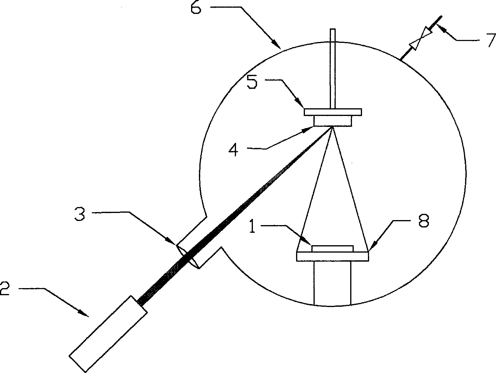
[0043] b) will (ZrO 2 ) 0.5 (SiO 2 ) 0.5 The ceramic target 4 is fixed in a pulsed laser deposition film-making system (such as figure 1 On the target stage 5 shown in ), the silicon substrate 1 is fixed on the substrate stage 8, and they are all placed in the growth chamber 6 of the pulsed laser deposition film-making system;
[0044] c) Use a vacuum pump to evacuate the growth chamber 6 to 1.0×10 through the interface valve 7 of the mechanical pump and the molecular pump -4 ...
Embodiment 2
[0047] Embodiment 2. High dielectric constant (ZrO 2 ) 0.8 (SiO 2 ) 0.2 The preparation method of thin film, its preparation steps are as follows:
[0048] a) (ZrO 2 ) 0.8 (SiO 2 ) 0.2 Ceramic target 4 is made of ZrO 2 , SiO 2 prepared by powder mixing solid phase sintering; in the ZrO 2 , SiO 2 After the powders are uniformly mixed at a molar ratio of 0.8:0.2, ball milled for 15 hours, then sintered at 1350°C for 4 hours, cooled to produce (ZrO 2 ) 0.8 (SiO 2 ) 0.2 Ceramic target 4;
[0049] b) will (ZrO 2 ) 0.8 (SiO 2 ) 0.2 The ceramic target 4 is fixed in a pulsed laser deposition film-making system (such as figure 1 On the target stage 5 shown in ), the silicon substrate 1 is fixed on the substrate stage 8, and they are all placed in the growth chamber 6 of the pulsed laser deposition film-making system;
[0050]c) Use a vacuum pump to evacuate the growth chamber 6 to 1.0×10 through the interface valve 7 of the mechanical pump and the molecular pump -...
Embodiment 3
[0053] Embodiment 3. Use high dielectric constant (ZrO 2 ) x (SiO 2 ) 1-x The preparation method of the non-volatile memory memory element of the thin film, the specific preparation steps are as follows:
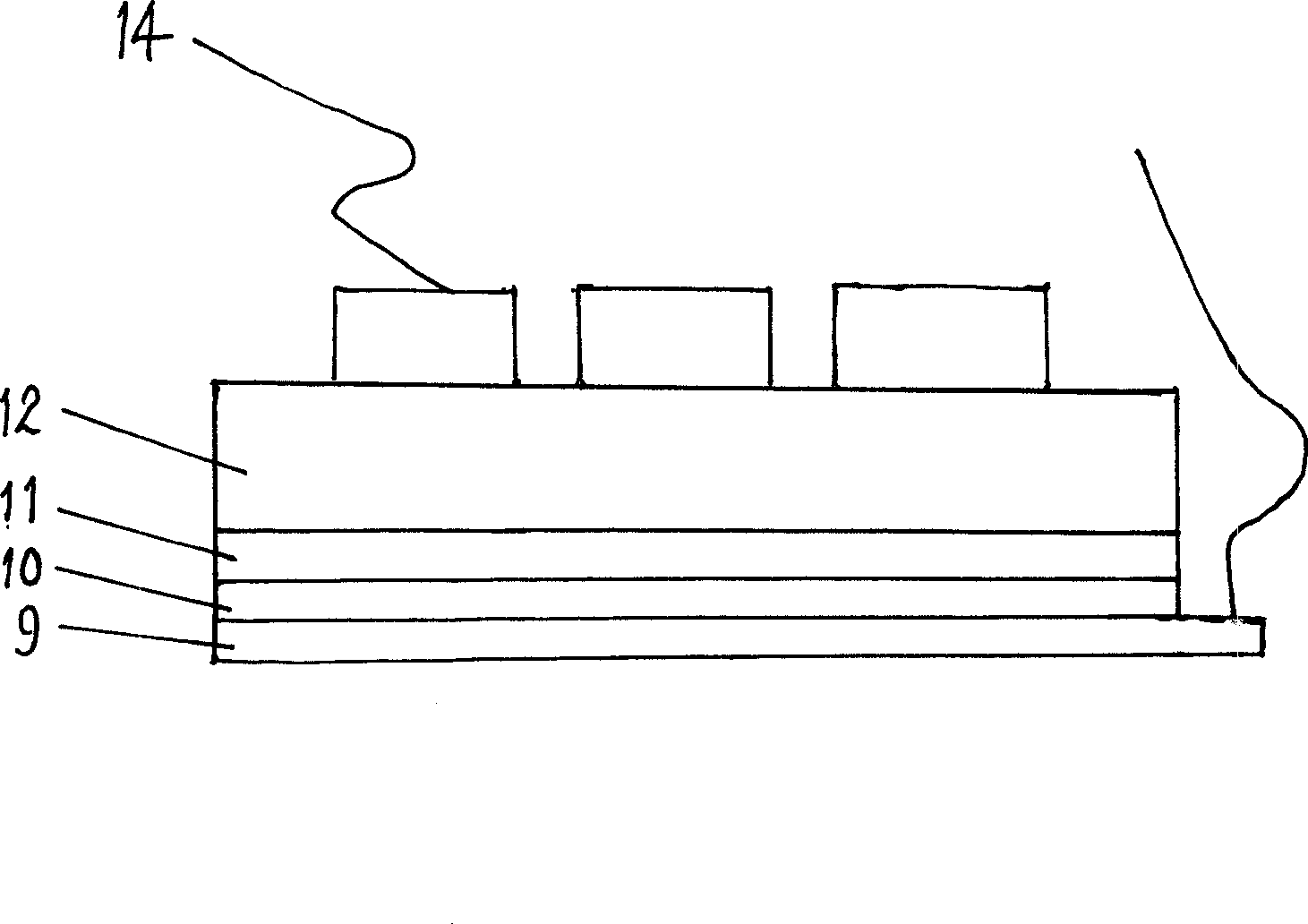
[0054] 1) Deposit a high dielectric constant (ZrO 2 ) 0.5 (SiO 2 ) 0.5 The thin film tunneling layer 10 has a thickness of 2-3 nanometers;
[0055] 2) In high dielectric constant (ZrO 2 ) 0.5 (SiO 2 ) 0.5 A layer of easily crystallized (ZrO 2 ) 0.8 (SiO 2 ) 0.2 A thin-film charge storage layer 11 with a thickness of 1-1.5 nanometers;
[0056] 3) Easy to crystallize (ZrO 2 ) 0.8 (SiO 2 ) 0.2 A layer of high dielectric constant (ZrO 2 ) 0.5 (SiO 2 ) 0.5 Thin film barrier layer 12, its thickness is 10-15 nanometer;
[0057] 4) Memory element at 800°C N 2 Medium rapid thermal annealing treatment for 5 minutes;
[0058] 5) Deposit the electrode film 13 on the above-mentioned memory element by magnetron sputtering on the stainless steel metal mask, the ma...
PUM
| Property | Measurement | Unit |
|---|---|---|
| wavelength | aaaaa | aaaaa |
| energy | aaaaa | aaaaa |
| energy density | aaaaa | aaaaa |
Abstract
Description
Claims
Application Information


