
Zirconium silicon oxide thin film with high dielectric coefficient, and preparation and use thereof

A high dielectric constant, silicon-oxygen technology, used in the field of microelectronic materials

Inactive Publication Date: 2011-07-20
NANJING UNIV
View PDF2 Cites 2 Cited by
  • Summary
  • Abstract
  • Description
  • Claims
  • Application Information

AI Technical Summary

Problems solved by technology

The currently used non-volatile memory magnetic media storage cannot achieve fast reading and writing due to the mechanical relative movement of the magnetic head and the recording medium during the reading and writing process.
Electronic storage technologies such as Flash do not require mechanical components, but due to the use of thicker tunneling layers, they have disadvantages such as high operating voltage and relatively slow read and write speeds.
In addition, there are ferroelectric memory (FeRAM) under research, M-RAM based on spintronic materials, etc., which have not yet been widely used due to some of their weaknesses

Method used


Image

  • Zirconium silicon oxide thin film with high dielectric coefficient, and preparation and use thereof
  • Zirconium silicon oxide thin film with high dielectric coefficient, and preparation and use thereof
  • Zirconium silicon oxide thin film with high dielectric coefficient, and preparation and use thereof

Examples


Embodiment 1

[0043] Embodiment 1. High dielectric constant (ZrO 2 ) 0.5 (SiO 2 ) 0.5 The preparation method of thin film, its preparation steps are as follows:

[0044] a) (ZrO 2 ) 0.5 (SiO 2 ) 0.5 Ceramic target 4 is made of ZrO 2 , SiO 2 prepared by powder mixing solid phase sintering; in the ZrO 2 , SiO 2 After the powders are evenly mixed at a molar ratio of 0.5:0.5, ball milled for 18 hours, then sintered at 1400°C for 5 hours, cooled to make (ZrO 2 ) 0.5 (SiO 2 ) 0.5 Ceramic target 4;

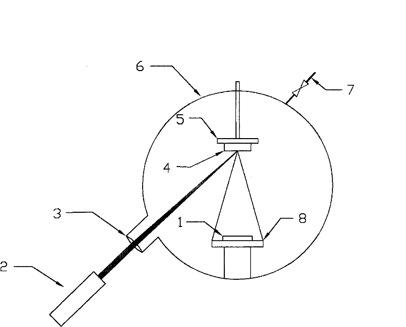
[0045] b) will (ZrO 2 ) 0.5 (SiO 2 ) 0.5 The ceramic target 4 is fixed in a pulsed laser deposition film-making system (such as figure 1 On the target stage 5 shown in ), the silicon substrate 1 is fixed on the substrate stage 8, and they are all placed in the growth chamber 6 of the pulsed laser deposition film-making system;

[0046] c) Use a vacuum pump to evacuate the growth chamber 6 to 1.0×10 through the interface valve 7 of the mechanical pump and the molecular pump -4 Bel...

Embodiment 2

[0049] Embodiment 2. High dielectric constant (ZrO 2 ) 0.8 (SiO 2 ) 0.2 The preparation method of thin film, its preparation steps are as follows:

[0050] a) (ZrO 2 ) 0.8 (SiO 2 ) 0.2 Ceramic target 4 is made of ZrO 2 , SiO 2 prepared by powder mixing solid phase sintering; in the ZrO 2 , SiO 2 After the powders were evenly mixed at a molar ratio of 0.8:0.2, ball milled for 15 hours, then sintered at 1350°C for 4 hours, cooled to produce (ZrO 2 ) 0.8 (SiO 2 ) 0.2 Ceramic target 4;

[0051] b) will (ZrO 2 ) 0.8 (SiO 2 ) 0.2 The ceramic target 4 is fixed in a pulsed laser deposition film-making system (such as figure 1 On the target stage 5 shown in ), the silicon substrate 1 is fixed on the substrate stage 8, and they are all placed in the growth chamber 6 of the pulsed laser deposition film-making system;

[0052]c) Use a vacuum pump to evacuate the growth chamber 6 to 1.0×10 through the interface valve 7 of the mechanical pump and the molecular pump -4 ...

Embodiment 3

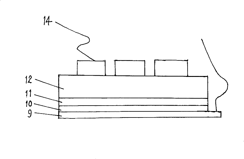
[0055] Embodiment 3. Use high dielectric constant (ZrO 2 ) x (SiO 2 ) 1-x The preparation method of the non-volatile memory memory element of the thin film, the specific preparation steps are as follows:

[0056] 1) Deposit a high dielectric constant (ZrO 2 ) 0.5 (SiO 2 ) 0.5 The thin film tunneling layer 10 has a thickness of 2-3 nanometers;

[0057] 2) In high dielectric constant (ZrO 2 ) 0.5 (SiO 2 ) 0.5 A layer of easily crystallized (ZrO 2 ) 0.8 (SiO 2 ) 0.2 A thin-film charge storage layer 11 with a thickness of 1-1.5 nanometers;

[0058] 3) Easy to crystallize (ZrO 2 ) 0.8 (SiO 2 ) 0.2 A layer of high dielectric constant (ZrO 2 ) 0.5 (SiO 2 ) 0.5 Thin film barrier layer 12, its thickness is 10-15 nanometer;

[0059] 4) Memory element at 800°C N 2 Medium rapid thermal annealing treatment for 5 minutes;

[0060] 5) Deposit the electrode film 13 on the above-mentioned memory element by magnetron sputtering on the stainless steel metal mask, the ma...


PUM

PropertyMeasurementUnit
wavelengthaaaaaaaaaa
energyaaaaaaaaaa
energy densityaaaaaaaaaa

Abstract

The invention discloses a novel memorization material on the basis of nanocrystalline high-dielectric coefficient (ZrO2)x(SiO2)[1-x] films, wherein, 0.2<=x<=0.9, and the materials can be used to prepare non-volatile memorization device and integrated circuits for information storage or other functions.The high-dielectric coefficient (ZrO2)x(SiO2)[1-x] films has the following characteristics that: when x is smaller, the films can remain amorphous after a high-temperature quick thermal annealing process; when x is bigger, ZrO2 nanocrystalline is partly crystallized and precipitated after the high-temperature quick thermal annealing process, simultaneously the film is a insulator with a high-dielectric coefficient and a large-forbidden band width, after substituting SiO2 by ZrO2, the size of devices is reduced and excellent insulativity is remained, therefore, a non-volatile memorization device with small size, high-density and stable performance can be prepared by using the films. The present invention provides method for preparing high-dielectric coefficient (ZrO2)x(SiO2)1-x films and the method comprises sintering ZrO2 and SiO2 with an appropriate proportion to produce ceramic target materials and preparing high-dielectric coefficient zirconium silica films by using a laser burst deposition method.

Description

technical field [0001] The invention belongs to the field of microelectronic materials, in particular to a (ZrO 2 ) x (SiO 2 ) 1-x Thin films and methods for their preparation. Background technique [0002] Memory systems currently used by computers include volatile memory and nonvolatile memory. The former is mostly used in the internal memory of the computer system, and cannot save data when there is no power support. The latter can completely save the original data when there is no power support, so it is widely used in data storage of electronic systems, such as computers, digital equipment, industrial control equipment, etc. Currently used non-volatile memory magnetic media storage cannot achieve fast reading and writing because the magnetic head and the recording medium need to move mechanically during the reading and writing process. Electronic storage technologies such as Flash do not require mechanical components, but due to the use of thicker tunneling layer...

Claims


Application Information

Patent Timeline
Patent Type & Authority Patents(China)
IPC IPC(8): C23C14/08C23C14/24G11B9/06
Inventor 殷江吕仕成夏奕东刘治国
Owner NANJING UNIV
Learn More