Photon crystal coupling narrowband response quantum well infrared detector

An infrared detector, photonic crystal technology, applied in semiconductor devices, optical waveguides, electrical components, etc., can solve the problems of low response and wide response band, and achieve the effect of suppressing the density of states, enhancing the density of states, and enhancing performance.

Inactive Publication Date: 2009-07-29
SHANGHAI INST OF TECHNICAL PHYSICS - CHINESE ACAD OF SCI
View PDF0 Cites 10 Cited by
  • Summary
  • Abstract
  • Description
  • Claims
  • Application Information

AI Technical Summary

Problems solved by technology

[0004] The purpose of the present invention is to provide a photonic crystal coupled narrowband response quantum well infrared detector, which solves the problem that the existing grating couple

Method used


Image

  • Photon crystal coupling narrowband response quantum well infrared detector
  • Photon crystal coupling narrowband response quantum well infrared detector
  • Photon crystal coupling narrowband response quantum well infrared detector

Examples


Embodiment Construction

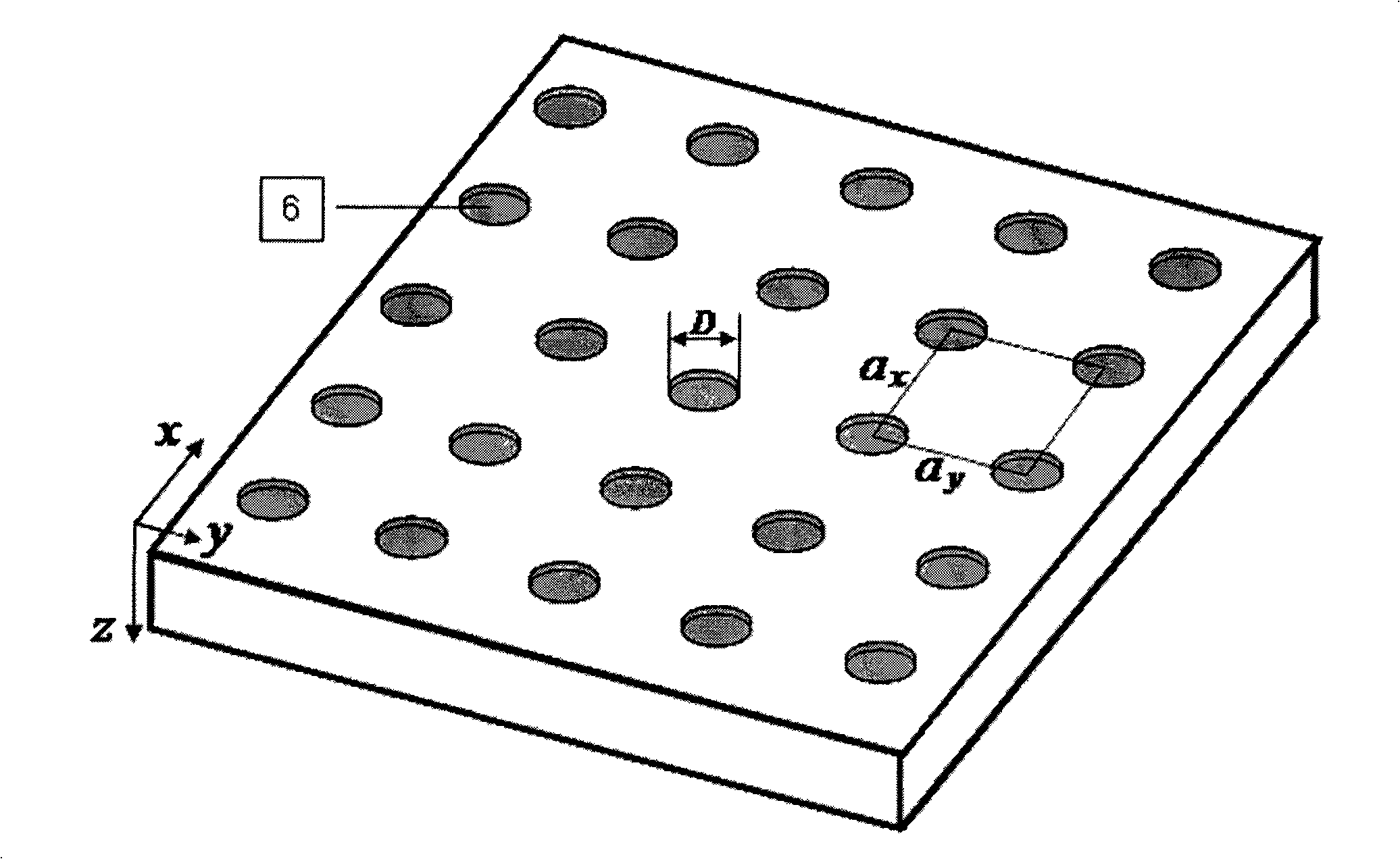
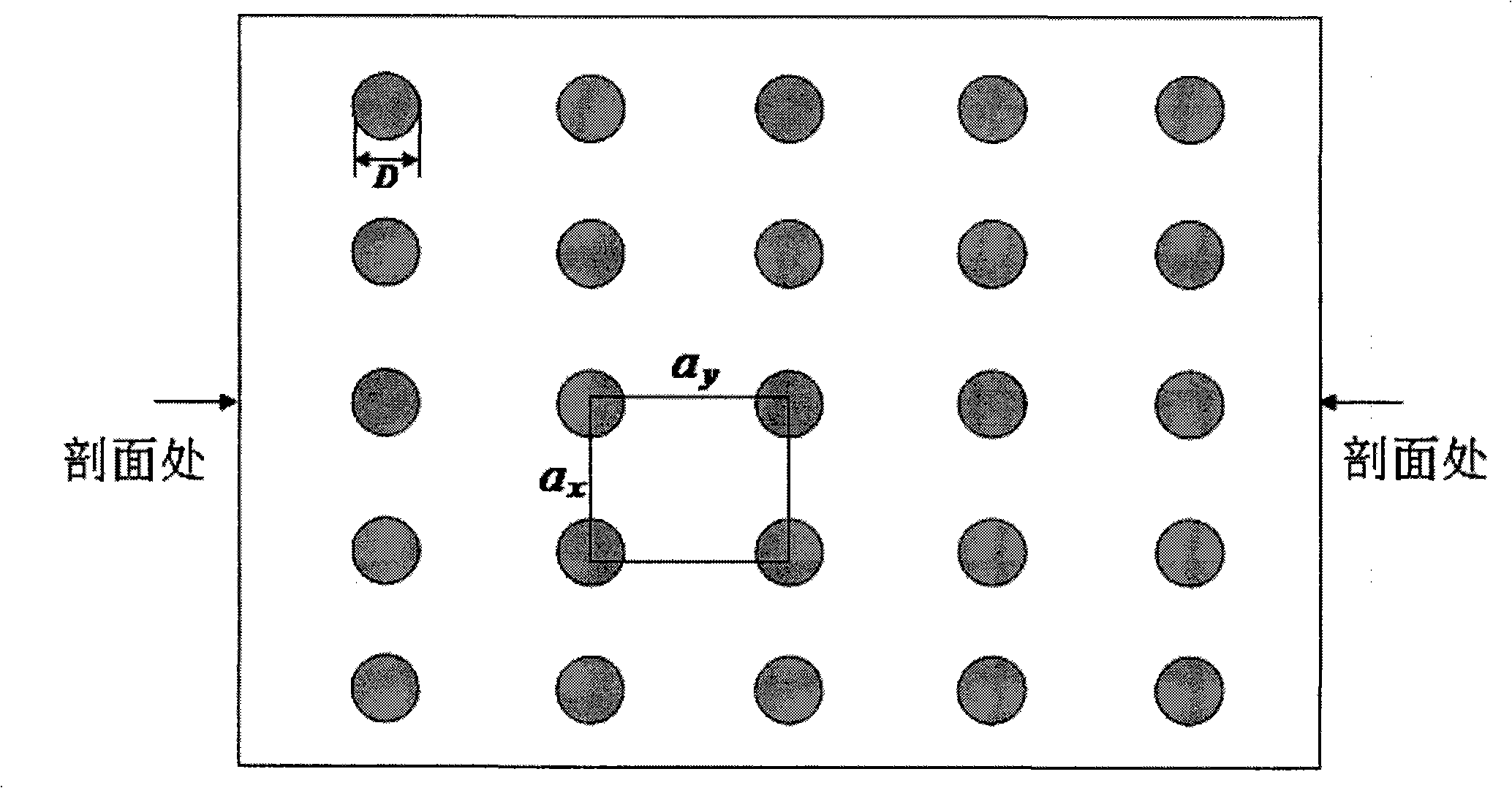
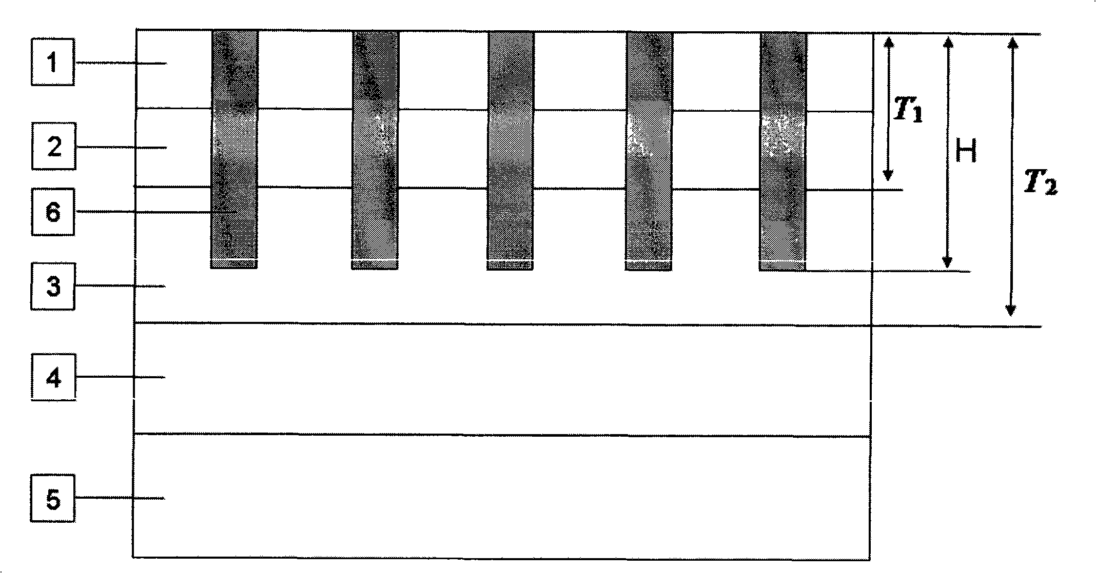
[0023] According to the technical solution of the present invention, we take the photonic crystal coupled narrowband response quantum well infrared detection unit with a peak response wavelength of about λ=15 μm as an example, and combine the attached figure 1 , 2 and 3 to illustrate the implementation of the device.

[0024] The GaAs / AlGaAs material of the present invention is grown by molecular beam epitaxy.

[0025] The said multi-quantum well layer has 50 periods in total, and each period includes a 60nm Al 0.15 Ga 0.85 As barrier layer and a 7nm GaAs quantum well layer, the doping concentration of the quantum well is 2.5×10 17 cm -3 ; The upper and lower emitters are n-type doped GaAs, the doping concentration is 2.5×10 17 cm -3 .

[0026] The thickness of the upper emitter n-type doped GaAs layer is 1 μm, Al 0.15 Ga 0.85 The thickness of the As barrier layer is 47nm, namely:

[0027] T 1 = 1.0 μm;

[0028] T 2 = 4.4 μm.

[0029] Use photolithography to etch...


PUM

PropertyMeasurementUnit
Diameteraaaaaaaaaa

Abstract

The invention discloses a quantum well infrared detector of a photonic crystal coupling narrowband response. A photonic crystal is combined with a quantum well infrared detecting unit; and the photonic crystal, as a coupling unit, is directly nested in the infrared detecting unit. The modulation of a periodic surface structure and the photonic crystal to photon state leads the response of the quantum well infrared detecting unit to specific wave bands to be strengthened, while the response to other wave bands is restrained, thus achieving the detection of narrow band. Compared with the traditional quantum well detector, the detector has the advantages as follows: firstly, response wave band is narrow. The detector can regulate the position of peak response wavelength through the regulation and control of the photonic crystal to the photon state and the self structure control of the quantum well; secondly, the detection efficiency of the peak wavelength is high. Due to the realization of the control of the photon state, the detection efficiency is improved; and thirdly, user-oriented design is facilitated. New design dimension is provided for the regulation and control of the photon state, thus being more convenient for optimizing the matching property of response wave band of product according to the needs of the users.

Description

technical field [0001] The invention relates to a long-wave infrared quantum well detector technology, in particular to a photonic crystal coupling narrowband response quantum well infrared detector. Background technique [0002] In the last two decades, with the rapid development of low-dimensional materials, the laboratory research and commercial development of quantum well infrared detectors are very active. Compared with traditional mercury cadmium telluride infrared detectors, quantum well detectors have the advantages of good material uniformity, mature device manufacturing technology, radiation resistance, and low cost. For focal plane array detectors, these advantages are manifested more obvious. At present, it is generally optimistic that GaAs / AlGaAs multi-quantum well detectors have considerable prospects in the application of long-wavelength bands. However, according to the transition selection rule of quantum mechanics, only the incident light whose electric ve...

Claims


Application Information

Patent Timeline
IPC IPC(8): H01L31/036G02B6/12
Inventor 陆卫林乐王健甄红楼李宁陈平平李天信李志锋陈效双
Owner SHANGHAI INST OF TECHNICAL PHYSICS - CHINESE ACAD OF SCI
Why Eureka
Try Eureka