Single-slice integrated micro-lens and its production method

A technology of micro-lens and monolithic integration, which is applied to the structural details of lenses, lasers, and semiconductor lasers, etc., can solve problems such as harsh processing conditions, inconspicuous optical coupling performance, and poor control of lens shape, and achieve improved integrity. Excellent performance and reliability, good collection effect, and complete lens shape

Active Publication Date: 2009-08-12
THE 13TH RES INST OF CHINA ELECTRONICS TECH GRP CORP
View PDF0 Cites 7 Cited by
  • Summary
  • Abstract
  • Description
  • Claims
  • Application Information

AI Technical Summary

Problems solved by technology

[0004] The above two types of micro-lens processing methods have their own advantages and disadvantages. Although the former has a large refractive index and good light-gathering effect, the processing conditions are harsh and the shape of the lens is not easy to control; The appearance is good, but since the photoresist coating on the surface or back of the chip will not be too thick, the curvature of the lens formed by heating and reflow is not enough, which is not obvious for improving the optical coupling performance, and the lens protrudes from the plane, so the reliability needs to be improved

Method used


Image

  • Single-slice integrated micro-lens and its production method
  • Single-slice integrated micro-lens and its production method
  • Single-slice integrated micro-lens and its production method

Examples


Embodiment Construction

[0021] The present invention is described in further detail below in conjunction with accompanying drawing:

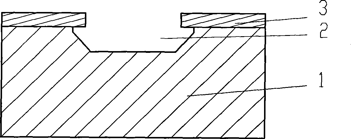
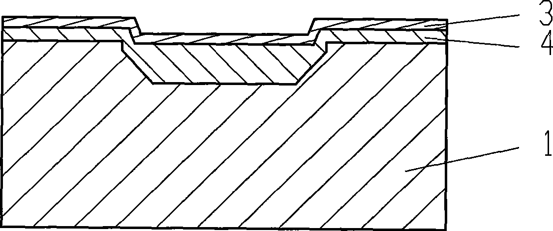
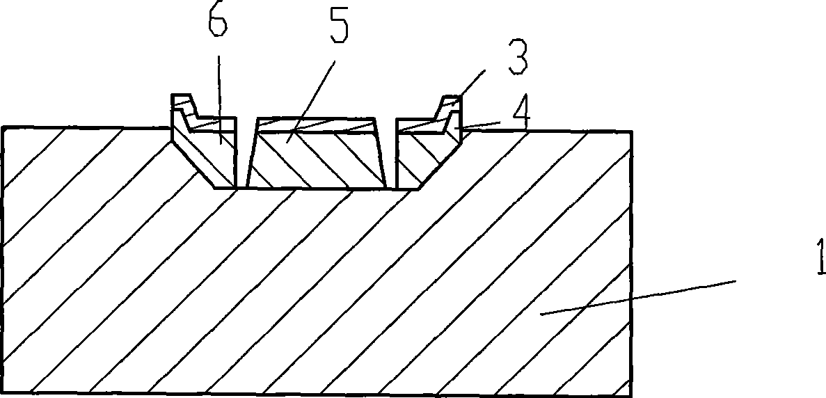
[0022] Such as figure 1 As shown, on an InP substrate 1, a pit 2 is etched by a wet etching process with a photoresist 3 as a mask.

[0023] The area and depth of the pits are adjusted according to the characteristics of the microlens.

[0024] The wet etching process adopts isotropic HBr, H 2 o 2 and H 2 O mixed solution, its volume ratio is 1:1:9, at room temperature (25°C), the corrosion rate is about 2 μm / min.

[0025] The pits can also be made by plasma dry etching process. Apply ICP etching equipment to adjust the reaction gas Cl 2 / CH 4 / H 2 The flow ratio is 7sccm:8sccm:5.5sccm, the incident power of radio frequency is 200W, the air pressure in the reaction chamber is 4-5mTorr, and a circular or square pit is made. By adjusting the reaction gas Cl 2 / CH 4 / H 2 The ratio of the ratio and the incident power of radio frequency and the air pressure in ...


PUM


Abstract

The invention discloses a single-element integrated microlens, which comprises a substrate and a microlens, and is characterized in that the microlens is positioned in a concave pit of the substrate and the method for manufacturing the microlens comprises the following steps: 1) forming the concave pit on one side of the substrate; 2) filling the concave pit with reflux photosensitive resist and then coating top layer masking photosensitive resist; 3) forming the photosensitive resist in the concave pit into a frustum shaped photosensitive resist column; 4) removing the top layer masking photosensitive resist; and 5) molting the photosensitive resist column by using a reflux process to form the microlens. Compared with the prior integrated microlens, the single-element integrated microlens has the characteristics of good lens shape, high entrenchment, batch production, and the like, and can be widely applied to light emitting tubes, lasers, photodetectors and other optical communication elements.

Description

technical field [0001] The invention relates to a method for manufacturing a single-chip integrated micro-lens, which belongs to the technical field of semiconductor micro-processing. Background technique [0002] With the rapid development of optical fiber communication technology, not only the demand for high-speed and high-performance optoelectronic devices is increasing, but also higher requirements are put forward for system performance such as high coupling efficiency and small tolerance. In light-emitting devices such as light-emitting diodes, It is a very effective means to make micro-lenses on the light-emitting surfaces of laser diodes and other light-receiving devices such as PIN photodetectors and MSM photodetectors, which can greatly improve the coupling efficiency of light and improve the coupling tolerance. . [0003] At present, the lenses used for semiconductor optical devices are mainly divided into two categories: one is externally configured, commonly kn...

Claims


Application Information

Patent Timeline
Patent Type & Authority Applications(China)
IPC IPC(8): G02B3/00H01L33/00H01S5/02H01S5/026H01L31/0232
Inventor 蔡道民李献杰曾庆明高向芝尹顺政赵永林
Owner THE 13TH RES INST OF CHINA ELECTRONICS TECH GRP CORP
Why Eureka
Try Eureka