Photoetching mask structure for aeration of X-ray and method for preparing same

A photolithography mask and X-ray technology, which is applied to the field of photolithography mask structure and preparation of X-ray exposure, can solve problems such as pattern distortion, and achieve the effects of reducing thermal deformation, simple process flow, and not easy to break

Inactive Publication Date: 2009-08-26
INST OF MICROELECTRONICS CHINESE ACAD OF SCI
View PDF0 Cites 11 Cited by
  • Summary
  • Abstract
  • Description
  • Claims
  • Application Information

AI Technical Summary

Problems solved by technology

But for graphics smaller than 100 nanometers, slight deformation will cause serious graphics distortion

Method used


Image

  • Photoetching mask structure for aeration of X-ray and method for preparing same
  • Photoetching mask structure for aeration of X-ray and method for preparing same

Examples


Embodiment Construction

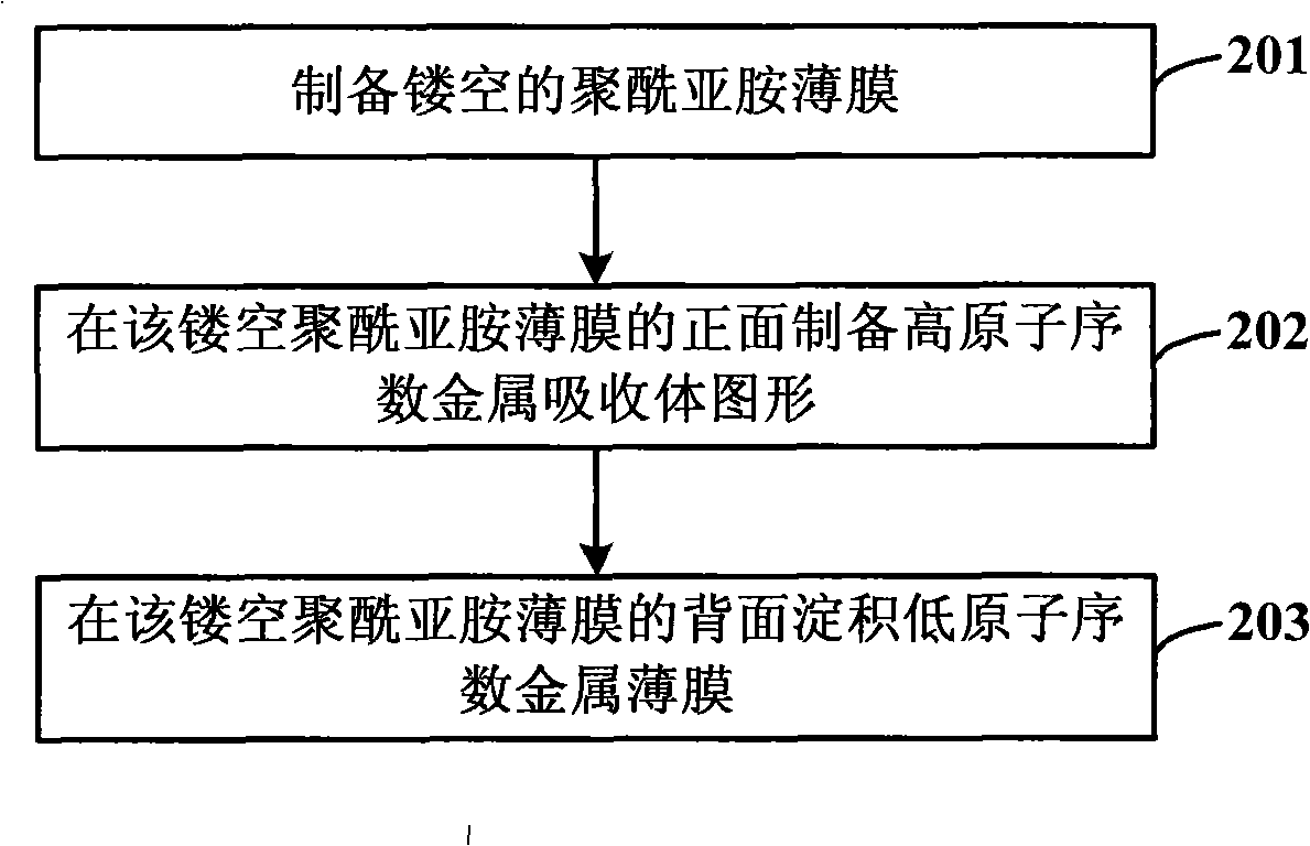
[0031] In order to make the object, technical solution and advantages of the present invention clearer, the present invention will be described in further detail below in conjunction with specific embodiments and with reference to the accompanying drawings.

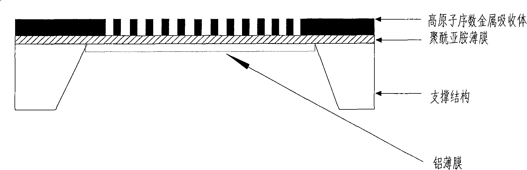
[0032] Such as figure 1 as shown, figure 1 A schematic cross-sectional view of a photolithographic mask structure for X-ray exposure provided by the present invention. The photolithographic mask structure is sequentially composed of low atomic number metal film, polyimide film and high atomic number metal absorber pattern from bottom to top.

[0033] The polyimide film is a hollow film with a thickness of 1 to 7 microns. The low atomic number metal film is formed on the back of the hollow polyimide film, generally an aluminum film, with a thickness of 100 to 200 nanometers. The high atomic number metal absorber pattern is formed on the front of the hollow polyimide film, which is a periodic, quasi-periodic and non-peri...


PUM

PropertyMeasurementUnit
Thicknessaaaaaaaaaa
Thicknessaaaaaaaaaa
Thicknessaaaaaaaaaa

Abstract

The invention discloses a photoetching mask structure for the aeration of X-ray. The structure, from the bottom to top, sequentially consists of a metallic film in low atomic number, a polyimide film and a metallic absorber figure in high atomic number. The invention simultaneously discloses a method for preparing the photoetching mask structure. By utilizing the method, because of the adoption of the multi-layer film structure formed by metal aluminum in low atomic number, the polyimide and the metallic absorber in high atomic number, the photoetching mask structure can be used for the X-ray photoetching on the level of micron, deep submicron and nanometer. Compared with the inorganic film based mask, the photoetching mask structure has the advantages of low cost, simple process flow and difficult cracking; and compared with the organic film based mask, the photoetching mask structure has the advantages of high mechanical strength, hard deformation and good heat conducting performance.

Description

technical field [0001] The invention relates to the fields of microelectronics, nano-processing and X-ray photolithography, in particular to a photolithography mask structure for X-ray exposure and a preparation method thereof. Background technique [0002] X-ray lithography plays an important role in microelectronics, nanofabrication and X-ray optics. Using deep submicron and even nanometer X-ray lithography technology, various practical devices have been manufactured, such as high-frequency T-gate compound semiconductor devices, surface acoustic wave sensors, and high-aspect-ratio X-ray diffraction optical elements. [0003] In the development of X-ray lithography, the development of X-ray mask has always been an important part of X-ray lithography technology. The X-ray lithography mask is a hollow film formed by light element materials with low atomic number (polyimide, SiNx, SiC, and diamond, etc.) and a high atomic number metal absorber (such as gold, tungsten, and tan...

Claims


Application Information

Patent Timeline
IPC IPC(8): G03F1/14G03F7/20G03F1/22
Inventor 朱效立谢常青叶甜春刘明
Owner INST OF MICROELECTRONICS CHINESE ACAD OF SCI
Why Eureka
Try Eureka