

Manufacturing method of AlGaN-based uv-LED device on SiC substrate
A manufacturing method and technology for LED devices, which are applied in electrical components, circuits, semiconductor devices, etc., can solve the problems of large light loss in the middle, long exit path, and much ultraviolet light absorption, so as to improve output power, improve exit aperture, process simple effect
Inactive Publication Date: 2010-12-01
XIDIAN UNIV
View PDF1 Cites 0 Cited by
- Summary
- Abstract
- Description
- Claims
- Application Information
AI Technical Summary
Problems solved by technology
In 2004, a 250nm LED was produced. The maximum power of a 200μ×200μ chip is close to 0.6mW, but the external quantum efficiency is only 0.01%.
As the emission wavelength decreases, the bottom buffer layer absorbs more and more ultraviolet light, which seriously affects the output light power and external quantum efficiency.
At present, the quality of the epitaxial layer is mainly improved by improving the structure of the device. However, the existing technology of emitting light from the bottom still has great shortcomings. The external quantum efficiency is too low; the second is that the crystal quality of the bottom AlN buffer layer is poor, resulting in an increase in the non-radiative recombination center of the material, which absorbs more ultraviolet light; the third is that the bottom buffer layer captures photons under the action of electrical stress. Defects increase, seriously affecting the reliability of the device
Method used
View moreImage
Smart ImageViewing Examples

Examples
Embodiment 1
Embodiment 2
Embodiment 3
Login to View More PUM
| Property | Measurement | Unit |
|---|---|---|
| power | aaaaa | aaaaa |
| power | aaaaa | aaaaa |
Abstract
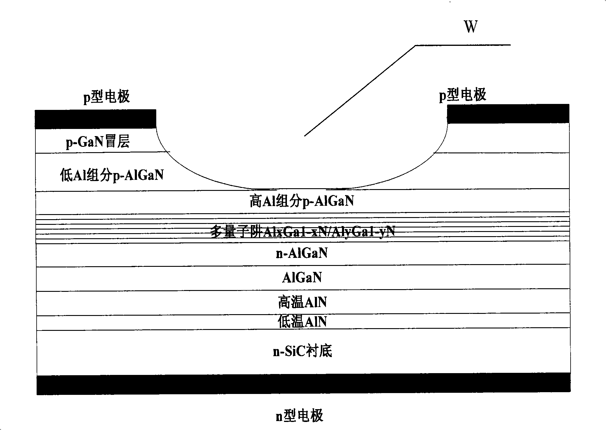
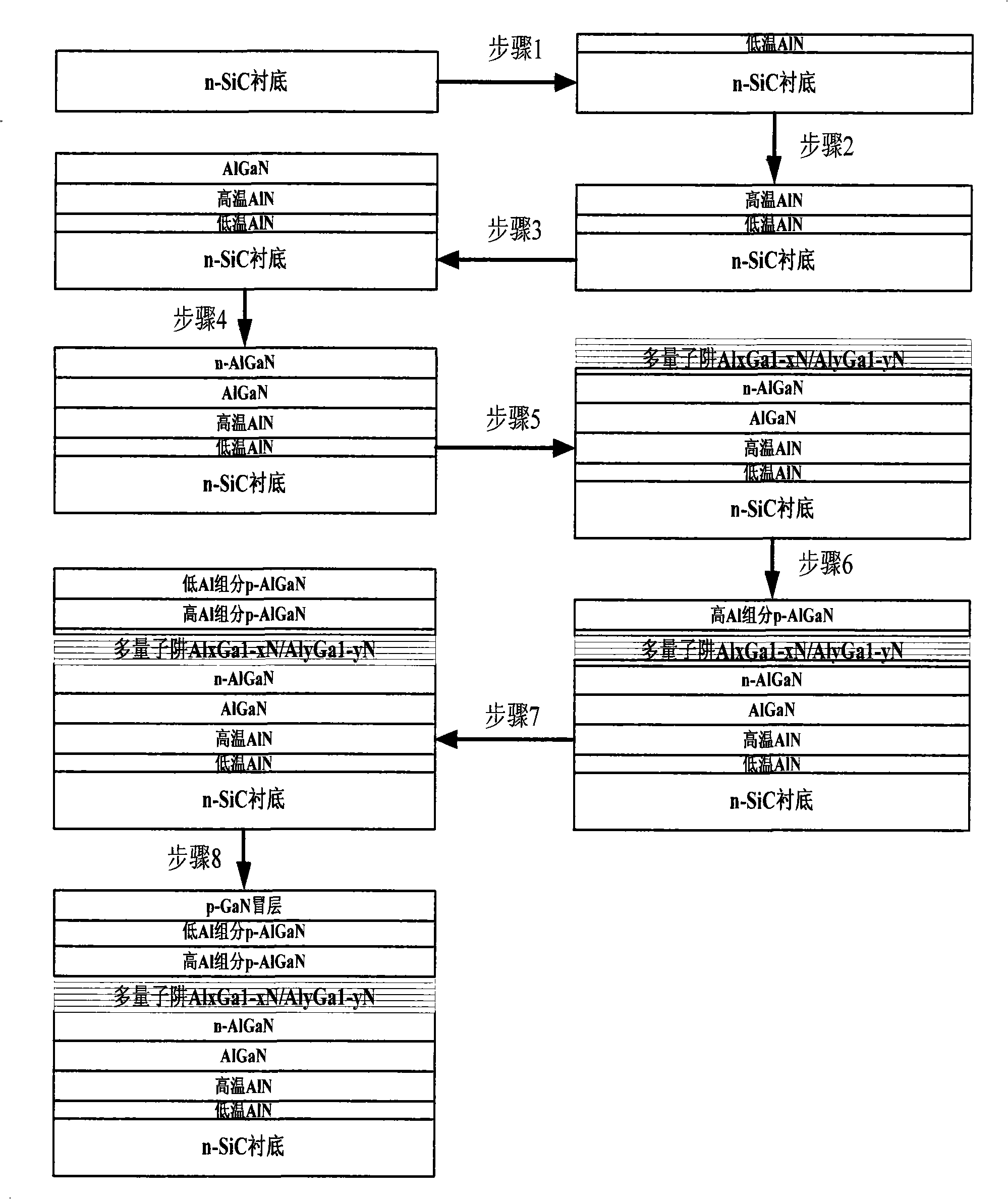
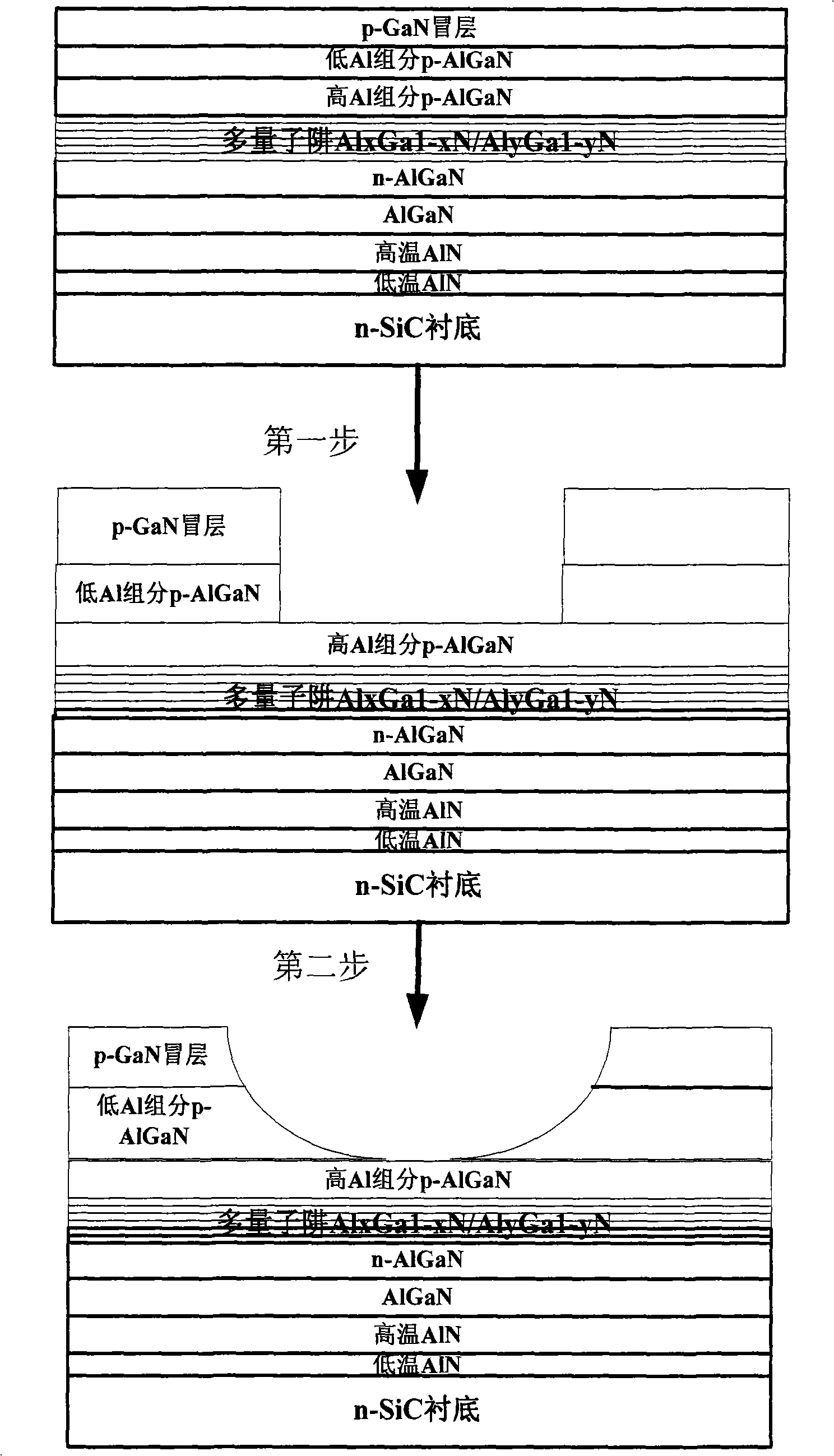
The invention discloses an AlGaN-based uv-LED device on a SiC substrate and a manufacturing method, relating to the technical field of micro-electronics and mainly solving the problem of low light-emitting efficiency. The device comprises a low-temperature AlN nucleating layer, a high-temperature AlN nucleating layer, an intrinsic AlGaN epitaxial layer, an n-AlGaN barrier layer, an active area, ap-AlGaN barrier layer, a low Al component p-shaped AlGaN layer, a p-shaped GaN capping layer and a window area arranged on the p-shaped GaN capping layer from bottom to top in sequence. The device etches the p-GaN capping layer to the low Al component p-AlGaN layer by a dry method to form a cylindrical emergent light window, and then the cylindrical emergent light window is etched by a photo-assisted wet method to be changed into a hemispheric-like window, so that the emergent aperture of the window is enlarged, the power and efficiency of the emergent light are improved and the window is especially suitable for manufacturing large-power uv-LED. The device has simple process, good repeatability and high reliability and can be used for water processing, medical treatment, biomedicine occasion and white light illumination.
Description
Fabrication method of ultraviolet LED on AlGaN-based SiC substrate technical field The invention belongs to the technical field of microelectronics and relates to a semiconductor device, in particular to a method for realizing a novel AlGaN-based multi-quantum well uv-LED device, which can be used in the fields of water treatment, medical treatment, biomedicine and white light illumination. Background technique As an outstanding representative of the third-generation semiconductor materials, III-V compound semiconductor materials have many excellent characteristics, especially in optical applications. The alloy {Ga(Al,In)N} composed of Ga, Al, In, N Can cover the entire visible light region and near ultraviolet light region. Moreover, the group III nitrides with wurtzite structure have direct band gaps, which are very suitable for the application of optoelectronic devices. Especially in the ultraviolet region, the AlGaN-based multi-quantum well uv-LED has shown great adva...
Claims
Login to View More Application Information
Patent Timeline
 Patent Type & AuthorityPatents(China)
IPC IPC(8): H01L33/00
Inventor郝跃杨凌马晓华周小伟李培咸
OwnerXIDIAN UNIV